Audio DAC mods
The current setup
This page is about the mods I'm looking to do on my DAC, a JEC TC-7500. I bought this item off e-bay for around £5 in 2009 or so and since then I have been using it quite happily as part of my Hi-Fi setup. I have no complaints about the sound quality, which is why I have used it for more than 10 years without making any changes to it.
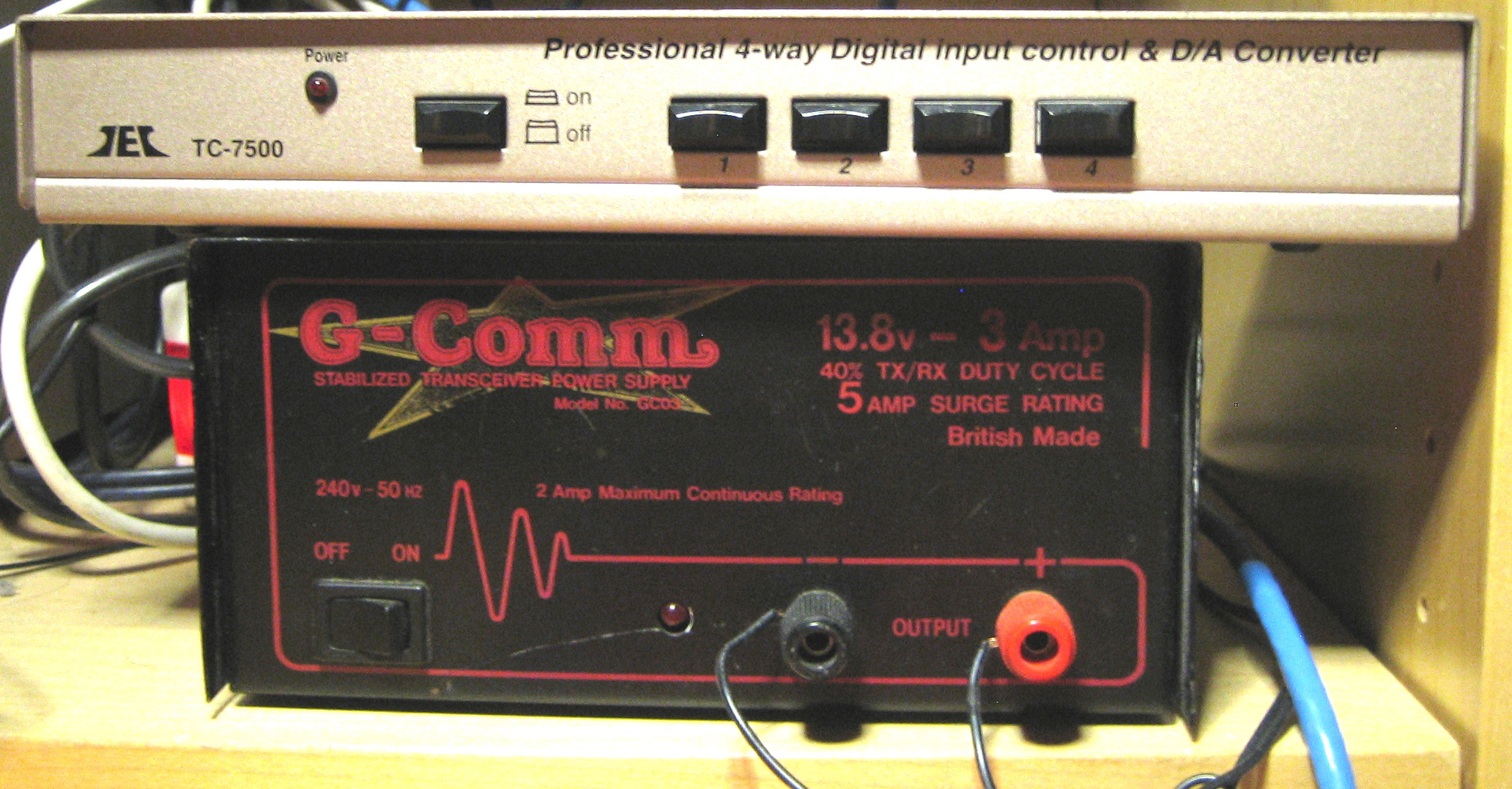
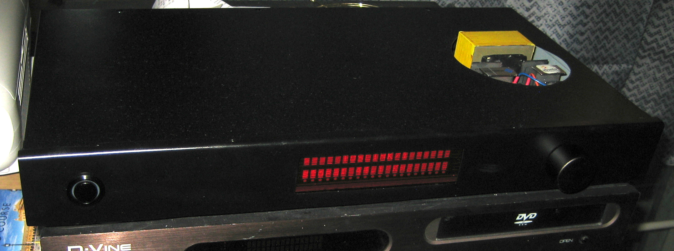
Here is my DAC in all its glory, sitting on top of its power supply:
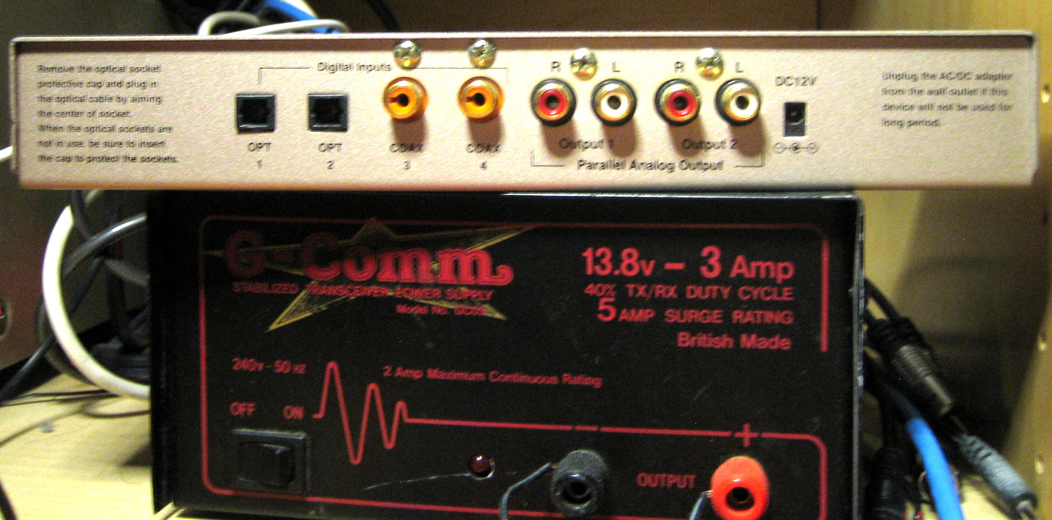
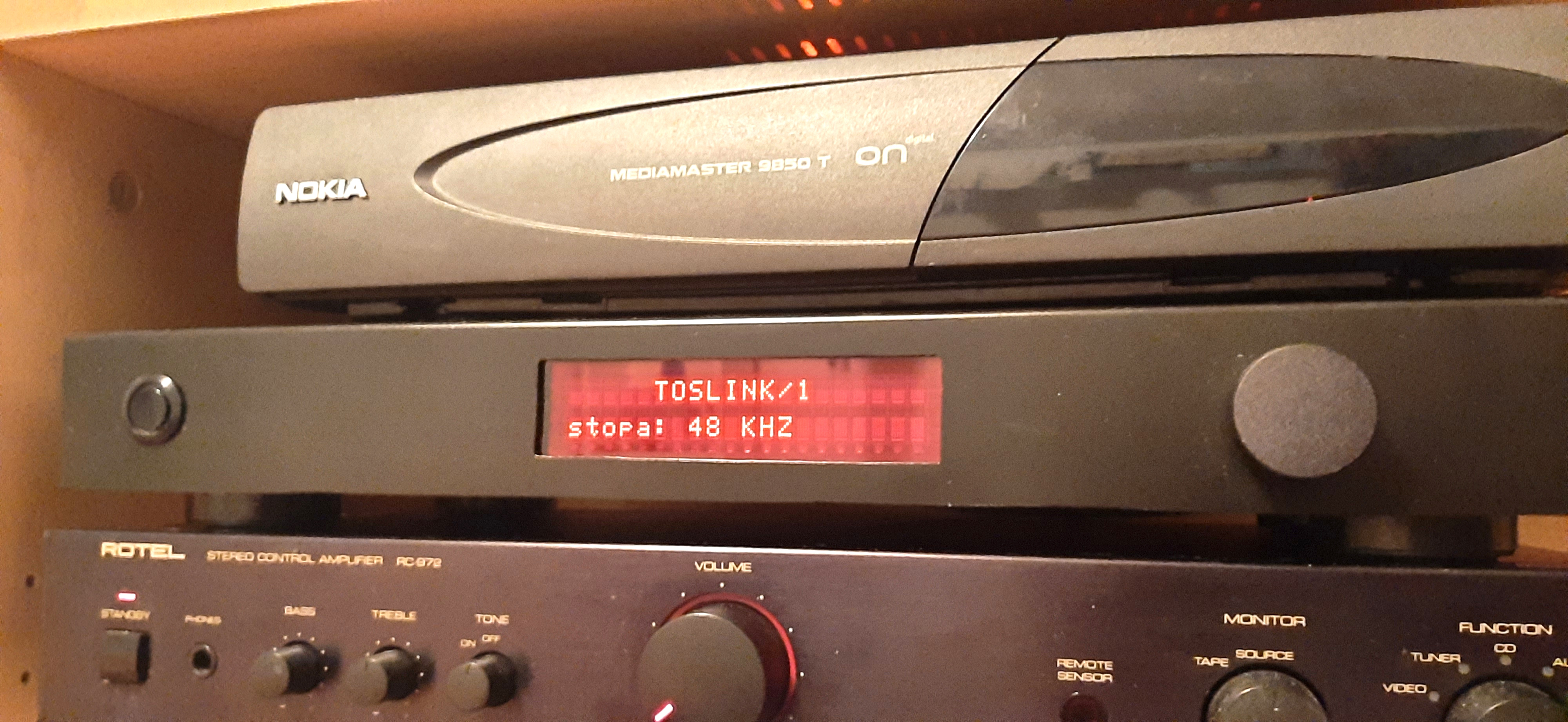
It has 4 inputs: 2x TOSLINK and 2x COAX and two mirrored analogue outputs:
So why this page about modding if I am happy with the DAC? Well, as you can see on the photos, the DAC does not have its own power supply. So it needs an external power supply unit. Also, the better the power supply, the better the audio quality. I originally used a general 12v "power brick" type supply, from my box of old power adaptors. It worked, but I noticed noise in the background. I replaced the power brick with another e-bay special, the G-Comm HAM Radio PSU (model GC03) for £3.99. This was much better, lowering the noise floor in the audio output, however on some occasions, when I turn on the power I get a large pop from the speakers, or the DAC just hisses and needs to be power cycled again before it works.
In addition, the PSU and DAC are not in a standard Hi-Fi format (or studio 19 inch rack format), so it sits off to the side of my Hi-Fi and it would be nice to put it in a case that would go with the rest of the Hi-Fi.
Mod plans
So, here is what I am currently planning to do with the setup
- Discover cause of popping and hissing when powered on from time to time and remedy if possible
- Provide more modern interface, ideally with some way of signalling details (e.g. sample frequency)
- Provide unified case for PSU and DAC
Stage 1: DAC Disassembly
Before I can begin with the mods, I need to know what I have to work with. I have not been able to find much information about this DAC on the internet, so I don't even know what DAC chip it uses internally.
The only relevant links that came up about the DAC are from the head-fi.org forum, specifically:
- this one from the head-fi forums and it is quite sparse on details.
- This more detailed post, from 2006
The second link has far more detail and the text description seems to match what my DAC has. However the photos don't match and the make on the forum posts is "Beresford", while mine is "JEC". Problem is that two different makes seem to use the TC-75XX model number and most of them are for the "Beresford". There is a link to http://www.homehifi.co.uk/products/TC-7500.htm on the forum, but that results in a 404, so I have no idea whether it is my DAC, or just a DAC that happens to have the same model number.
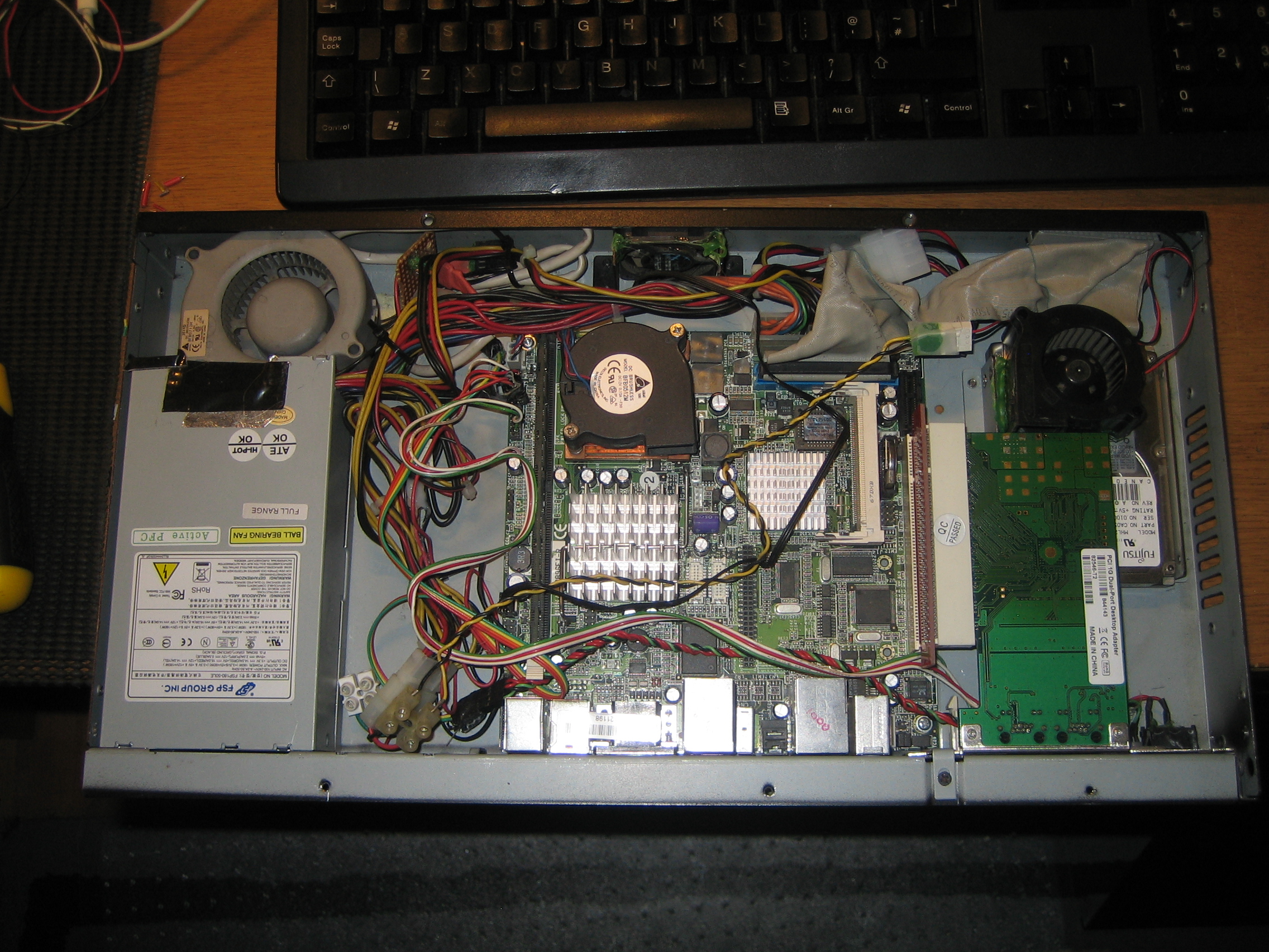
As such, there is only one thing for it. I have to disassemble my DAC and see what its innards look like. After flipping it around, you find four blind rivets holding it together, an odd setup as most equipment I've looked at used screws:
As such, I had to drill out the rivets, after which the case split easily in two. There is only one circuit board, with model markings
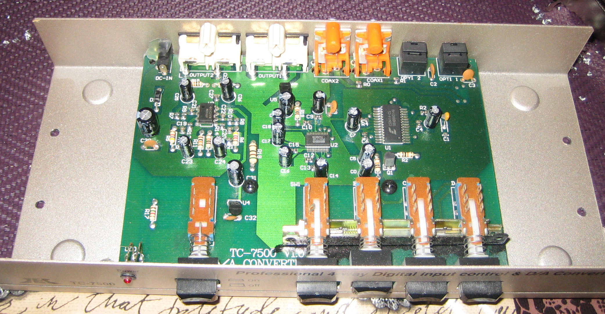
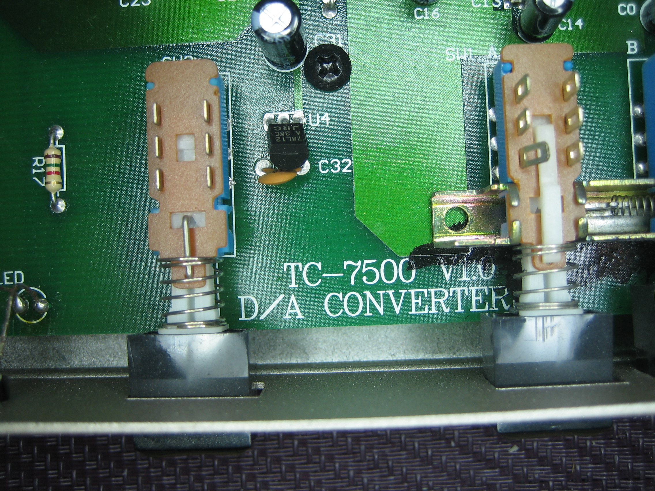
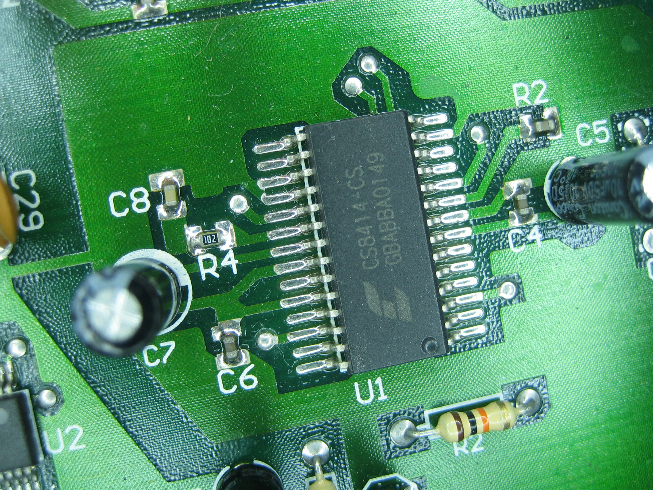
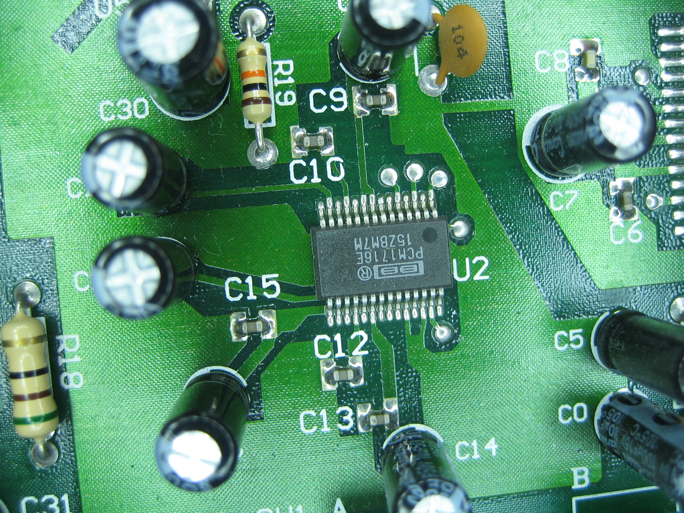
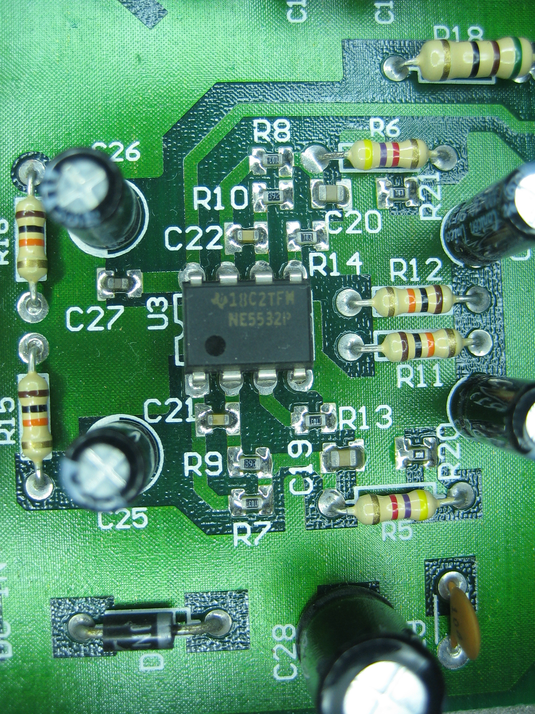
There are three main IC's on the PCB:
It looks like we have:
- A CS8414-CS - A Cirrus Logic (Crystal Semiconductor) Decoder/receiver (pdf data sheet)(Circa 1998)
- A PCM1716E - Burr Brown DAC (Multi-Level Delta-Sigma DAC, supports up to 24bit 96KHz audio frames, Circa 1997)
- A NE5532P - Low noise operational amplifier (A very long lived component. Released November 1979 and is still in production)
I have to say it has been a while since I saw a Cirrus Logic product, I remember them from the times of PC Graphics cards when I was still a kid. A bit of a nostalgia hit for me. Looking at the data sheet for this chip, I notice two things:
- That the chip is quite old, the data sheet is dated 1998. In fact all the chips I checked seem to be late 90s vintage, so this DAC itself may have been produced in the late 90s/early 00's
- That it is branded "Crystal, a division of Cirrus Logic". This is interesting to me, because the head-fi.org forum post I linked above mentioned a Crystal chip. Re-reading it, I find that the three chips are identical on the units. Now I don't know what the connection is between the JEC TC-7500 and the Beresford TC-7500/7510. They do seem to use the same components internally though.
The good news is that the components used in my DAC seem to be highly regarded for their sound quality, making my £5 purchase my second best audio bargain purchase after my power amplifier. As such it is a good unit to keep using. Likewise any modifications done will stay away from the audio path within the DAC. Analogue circuit design for audio applications is an art in of itself, so chances are the designers already did a far better job at it than I could do.
Interfacing to the CS8414 chip
Having had a look at the data sheet, there are two near identical CS chips. We have the CS8413 and the CS8414. The main difference is that the CS8414 is standalone, while the CS8413 needs a microcontroller to set it up. My DAC logically has the standalone version.
Good news is, that the CS8414 actually has parallel (7 multifunction pin) data outputs. You cannot control the chip, but you can read its status. If I could interface to this, I would be able to read input status from the chip.
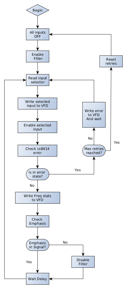
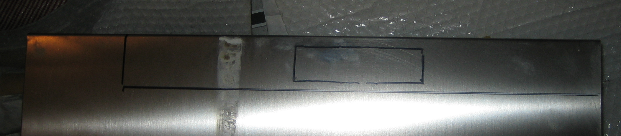
As the 7 multifunction pins would provide me with all the status info I would need, my first task would be to see if these pins are not already connected/in-use on the PCB. Below you see the chip pins:
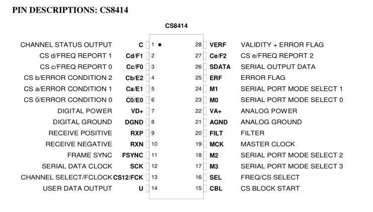
Here are the pin numbers overlaid on a rotated crop of the original photo
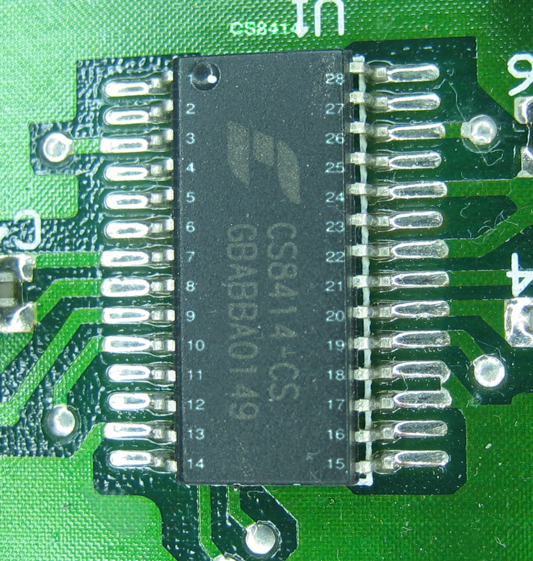
For extracting status information, we need pins 2-6,27 (E0,1,2 and F0,1,2) and 16 (SEL) free. Looking at the chip photo overlaid with numbers, all those pins are unused except pin 3. So we need to see what pin 3 is tied to and whether it is needed (they may have just tied it to ground).
Pin probing
So I got my trusty oscilloscope and multimeter and started tracing. Seems pin 3 goes to a transistor (Q1), of which one side is tied to ground and the other side goes off to the PCM1716E. Based on probing, it seems that this pin enables/disables some kind of audio filter. Most noticeably high frequencies are attenuated with the transistor is driven LOW. Also, white noise is eliminated when the pin is driven LOW. If you drive the pin HIGH and pick an input without any digital connection, you get a lot of noise, including high frequency sweeps and ringing. I suspect those are the oscillators in the IC. So pin 3 of the CS8414 switches this filter on and off, presumably so that when the DAC is powered with no digital input signal, you don't get a lot of noise through the speakers.
The next thing I found is that the SEL pin, despite not being connected to anything, has 5V across it. It seems that it defaults to HIGH and needs to be pulled LOW.
Looking at the data sheet for CS8414, is seems that when SEL is high (i.e. its default state), the multifunction outputs are sending the channel status and pin 3 acts as the "Cc" pin (also listed as "EM1" in the datasheet). When SEL is LOW, pin 3 acts as "F0", one of the pins that tell us the sample frequency.
Looking at EM1, is seems this is a status bit for "emphasis", table 8 "emphasis encoding" tells us that pin 3 is only HIGH when the signal has either "no emphasis", or "not indicated". The other two options (pin LOW) are for "CCITT J.17 emphasis" or "50/15 μs emphasis". Lacking knowledge, I did some quick research (especially as I only knew emphasis in the context of analogue audio noise reduction. No idea what it meant in the digital realm).
Two links have been used as reference:
-
Wikipedia entry This is interesting, because it references the "50/15 μs emphasis" directly, in this quote:
Although rarely used, there exists the capability for standardized emphasis in Red Book CD mastering. As CDs were originally intended to work on 14-bit audio, a specification for 'pre-emphasis' was included to compensate for quantization noise. After production specifications were instead set to 16 bits, quantization noise became less of a concern, but emphasis remained an option through standards revisions. The pre-emphasis is described as a first-order filter with a gain of 10 dB (at 20 dB/decade) and time constants 50 μs and 15 μs.
- 1996 vintage usenet posts on a website
This refers to "CCITT J.17" and from the first post, it tells us that this is for the AES/EBU interface, which is a professional standard. In fact it seems SPDIF was developed from it as a cheaper to implement consumer standard. If you ever used XLR balanced connectors for digital audio, that is the main use of AES/EBU.
So most likely the filter is a general "de-emphasis" filter, which is enabled when the signal calls for it and also when there is no signal input (presumably to supress noise as noted above). This is fine but it poses a problem for one of my mods. If I want to be able to discover the sample frequency of the source, I have to drive the SEL pin LOW, which changes what pin 3 is for, which may result in the filter being enabled/disabled at random points, affecting the sound output.
The only way to prevent this is to disconnect pin 3 from the transistor and use some logic to hold the value of EM1 while we drive SEL LOW, read the other status from the same pins, bring SEL high again and re-read EM1 value.
Stage 2: Popping and Hissing
Having completed the disassembly of the DAC unit and got a rough idea of how things work and what the pins are for, we can start debugging issues I am seeing, starting with the popping and hissing.
Sometimes when I turn on the power I get a really loud pop if the amp is already running. Also, sometimes I get hissing after power on rather than any sound.
My initial hypothesis with regards to the popping was spikes in the power delivery to the DAC. Easy way to test this was to keep the DAC turned on, but power cycle the PSU. Each time you would get a pop, but of varying loudness. However if I keep the PSU turned on, but just turn the DAC off and on, there is no such pop.
If I hook up the oscilloscope to the PSU and power it up, I notice that power does not start immediately, but rather there is a bit of a ramp, as the capacitors charge up.
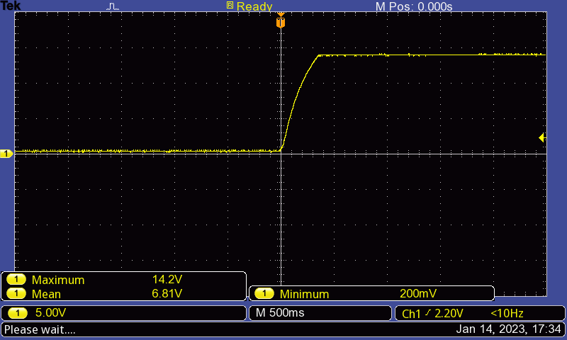
It is not much but it may be confusing the CS8414 chip, as during the ramp up the gradual voltage increase reaches a point where it can power the chip but not having it function properly.
If I add capacitance, the popping gets worse and the DAC just outputs noise (i.e. "hissing") more often from the audio stage. So it does seem related to the ramp up in voltage/inrush of current on initial start up.
Reading the CS8414 data sheet, It says:
The CS8414 should be reset immediately after power-up and any time the user issues a system wide reset.
In order to enact a chip reset, you have to pull M0, M1, M2 and M3 HIGH. Looking at this circuit, there is no reset implemented at all, most likely to save on components and cost. That may well be why we end up with the hissing from time to time. The chip is not in a clean state to decode the signal properly.
The circuit designer tied M1 HIGH and M2 + M3 LOW, while leaving M0 OPEN/NC (On table 3 of the data sheet, this indicates a mode setting of "In, L/R, 16-24 Bits") and didn't bother with the reset circuit. I suspect that was deemed acceptable by the chip designer, because I found out that if you either:
- Power cycle the DAC unit (from its power switch, i.e. no slow voltage ramp), or
- Switch input to something else, than back again
Then the hissing stops. Furthermore, if you deselect all inputs before you power on the DAC, power on and then select the input you want, it never hisses. I presume had I got the instruction manual when I bought this DAC it would have told me to not select an input until after the unit has powered on and "settled" a few seconds later. Probably much cheaper to add that line to the instructions than implement reset logic for the circuit.
Stage 3: Interface mods
Originally I would have liked to know what the sample frequency the DAC is running at. Nothing fancy, just 3 LEDS to indicate 32, 44.1 and 48Khz. However as noted above it is not as simple as reading some pins. We need to drive the SEL pin LOW, which in the design of this DAC would enable the de-emphasis filter and alter audio output. In addition this DAC is capable of more modes than I imagined, as it can handle up to 24-bit 96KHz audio frames.
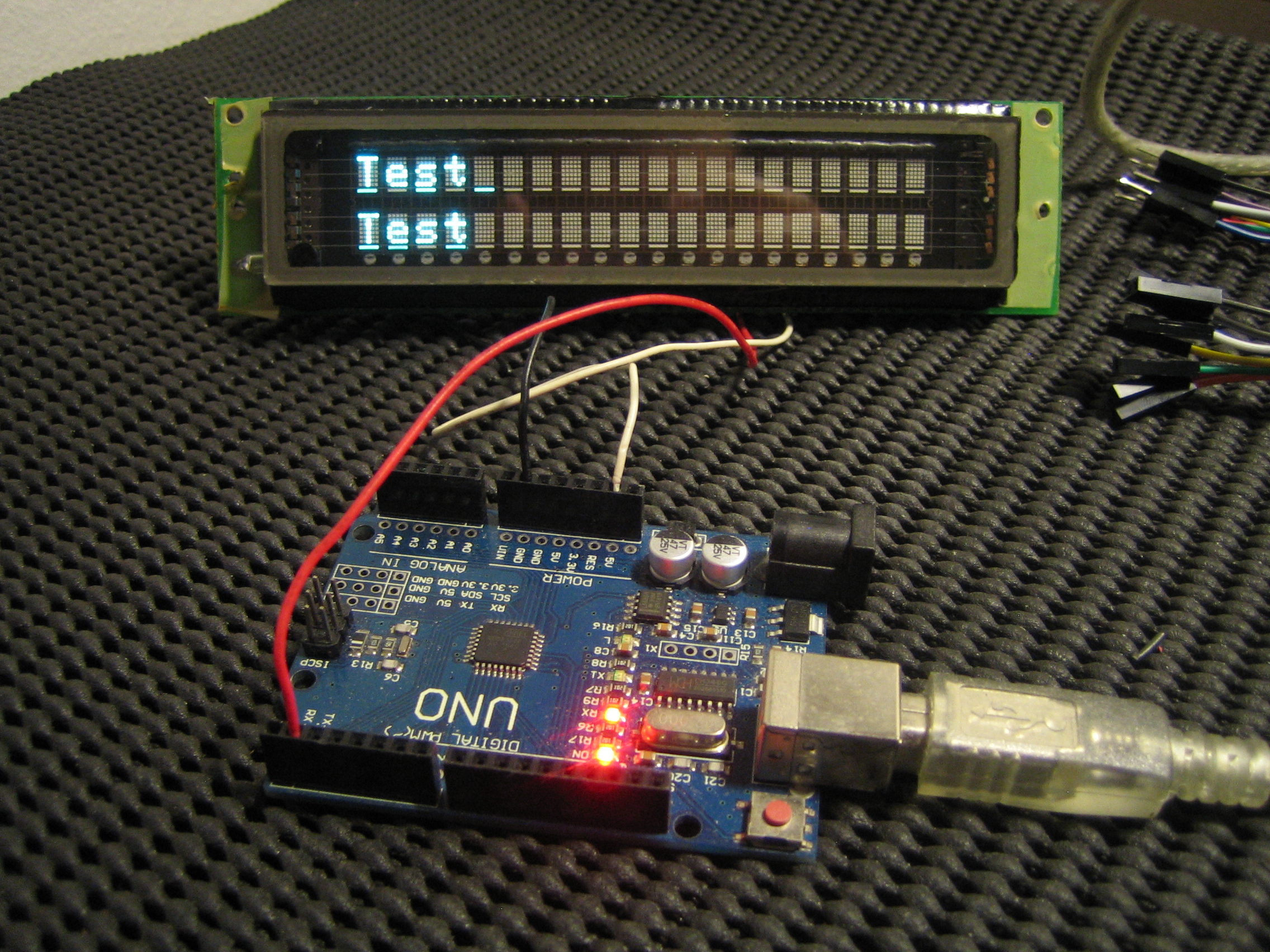
In order to keep the original audio filter/NR functionality but still be able to drive SEL low and read the pins, we need to latch it. We could make a discrete circuit to latch the audio stage power pin, read the status pins to another latch for the LEDs then revert, but I would rather use a microcontroller. Apart from requiring fewer components I can also do a lot more fancy things. Plus I have a pile of Arduinos sitting around just waiting for some use. In my components box I also have relays and LCD/VFD displays. So I might as well make use of all what I already have for the interface.
As such I am thinking of the following features for the interface:
- Power control, with the ability to delay the power until full voltage ramp up is done, to prevent popping
- Auto deselect all inputs and then select last used input after a delay, to prevent hissing
- Display of data stream information and input selection.
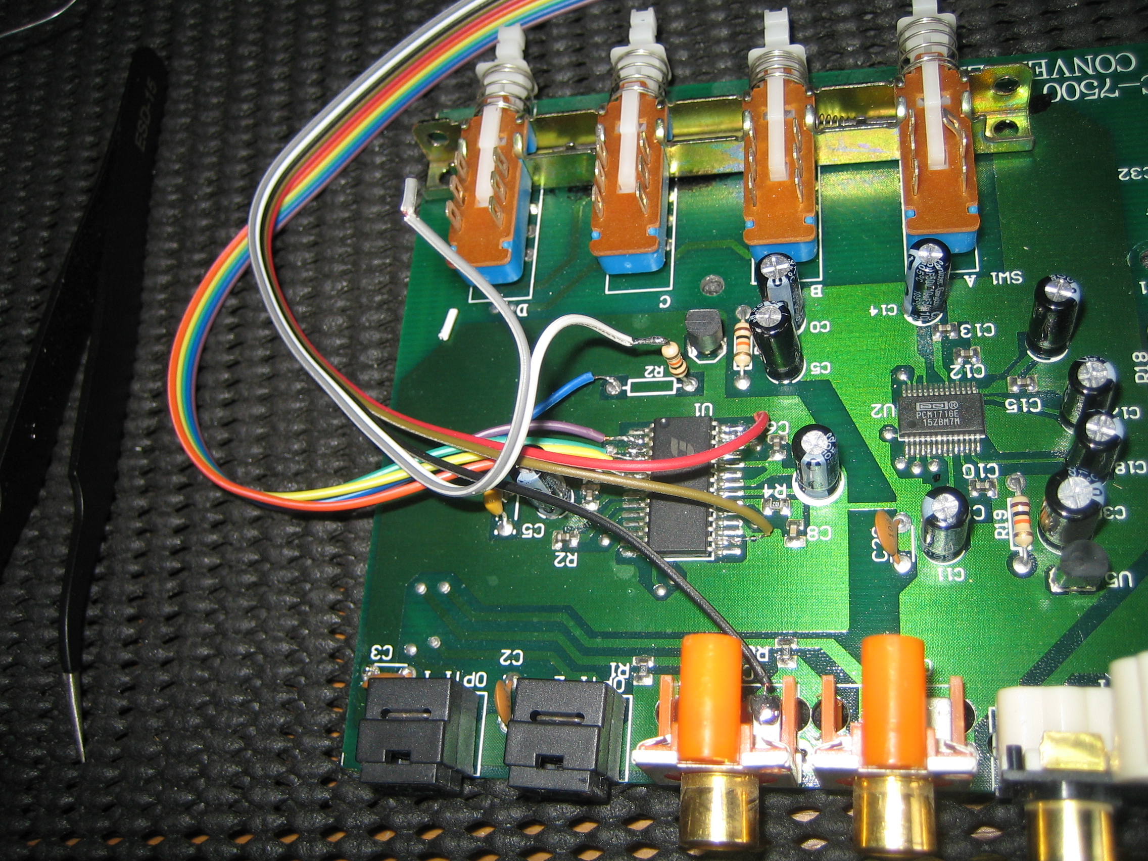
We have 4 inputs on the DAC, which use double pole double throw push switches with a mechanical interlock to prevent two inputs to be selected at once. To control them with relays I would ideally want 4 double pole double throw relays. However I already have an 8 channel power relay board, with single pole double throw relays.
I will tie two of the relays together to make a 4 channel double pole double throw system. This would allow 20A of current to flow through each input. Total and utter overkill and if I was to buy a component for this task, I would use something else. I bought these relays for a project that never was built in 2017 or so and at this point I would rather make use of it for something. In addition I had a choice to make about whether going solid state or relay based. Using transistors would risk signal degradation due to voltage drop across the transistor. While relays have the risk of debounce the fact the DAC already uses mechanical switches makes me think the circuit design has taken the debounce issue into account. Therefore to replicate the existing design as much as possible in an automated fashion using relays seems wiser.
So for the Arduino we would need:
- 4 output pins for the relay control board
- 1 output pin to latch audio stage power
- 1 output pin to drive SEL HIGH/LOW
- 6 input pins to read the chip error status and channel frequency
- 1 output pin to drive the power control to the entire DAC
- 2 output pins for the VFD Serial drive
At first glance, it would seem that we need 15 pins for this. However there are only 13 pins available on the Arduino Uno. For the moment we will not worry about this as it may turn out that we can save some pins somewhere during the development of this project. For now we will look primarily to getting the VFD up and running as that is in theory the simplest.
The VFD interface
The VFD we are to use is the Noritake Itron CU20026SCPB-T20A. HD44780 compatible, its main benefit is a built in serial interface, allowing a standard UART to drive it. As such we only need to use one pin of the Arduino for the VFD (look at that, we saved some pins already!). You can find its data sheet here.
Programming it was rather simple as it is standard serial interface. You just send bytes to it. A quick test message was implemented:
The Chip interface
I decided the second step should be to interface to the CS8414. This is the epitome of "Easier said than done" and is the most complex bit of this project so far. After much time (and some cursing), it was done.
I have never hand soldered a SOIC IC before and it was a real pain in the backside, especially making sure you don't accidentally bridge the pins. Lots of fiddling with tweezers, soldering, testing, checking for bridges (visual and continuity testing), then having to redo it when it went wrong. It was a very unpleasant experience and this is the biggest of the SOIC chips on the board. The smaller ones I don't think I could do at all. I doff my cap to those hobbyists that can solder BGA ICs at home. I'm quite happy never to move away from DIP ICs!
The next step was to solder to the Arduino pins, which was much easier. Once soldering was done basic logic was implemented in the Arduino to be able to read the frequency and error status from the chip and display it on the VFD. Currently just the raw bits were displayed for testing:
However it shows that we are correctly reading data from the chip. I plugged in my digital equipment and verified the sample rate. I also found out that almost all my equipment outputs 44.1KHz, regardless of the input source sample rate. Annoyingly it means they internally resample but there is nothing much I can do about that, at least the chip interfacing works!
The Relay interface
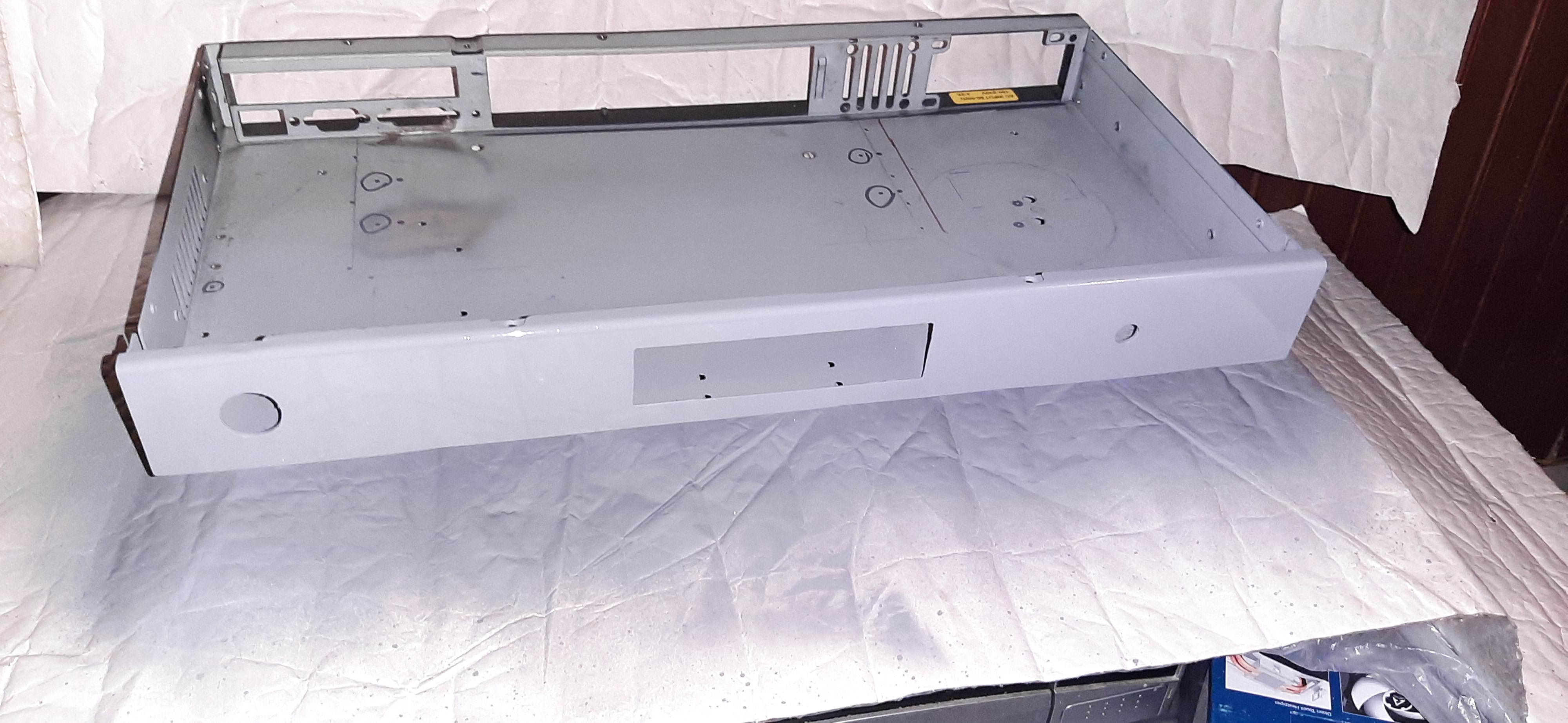
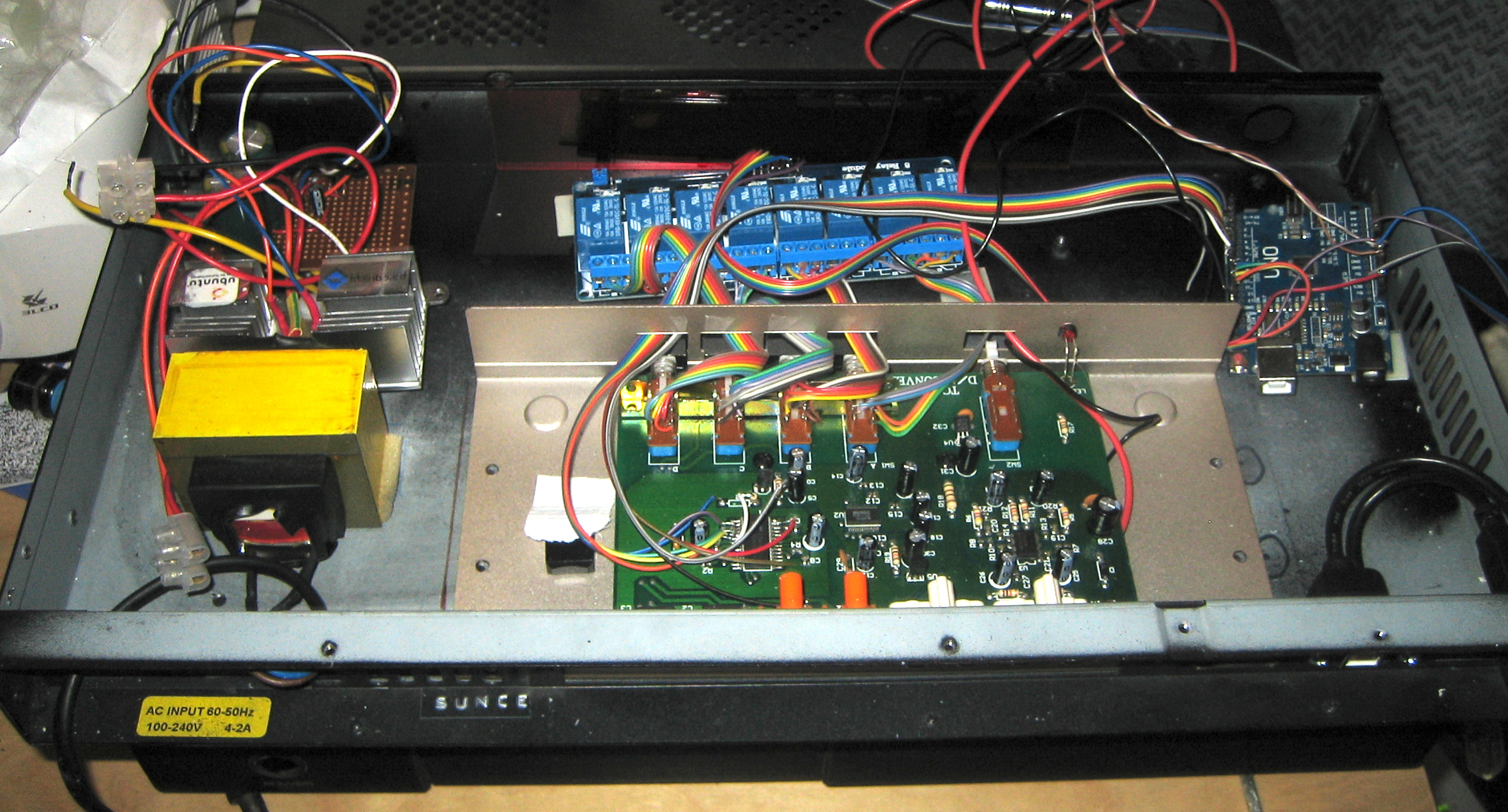
When it came to the relay interface it was also the time to start thinking about what enclosure I want to use and where to place the components, in order to know how long I need to make the wiring. So I had a rummage around my junk box and pulled out an old 1U server:
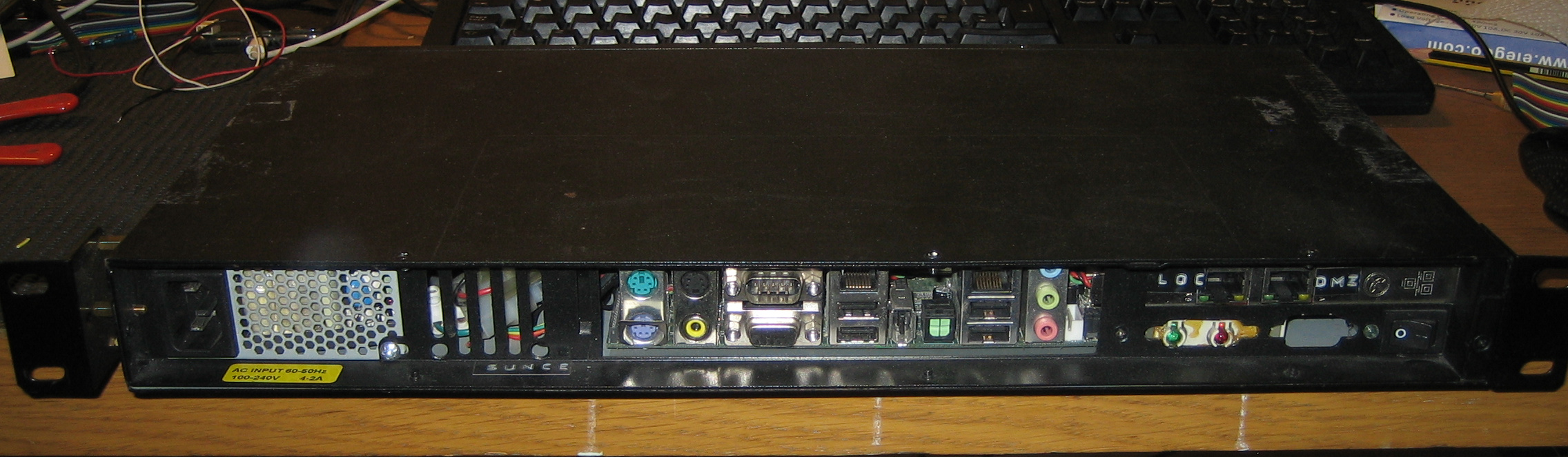
Those who have perused the rest of this site may recognise this as my old firewall. The fans were getting noisy and I managed to bag a proper 1U router/firewall combo for free near my workplace, so it has been replaced. I removed all the computer components and started placing my DAC components, looking at the optimum location for everything. After some fiddling, this is the best I came up with:
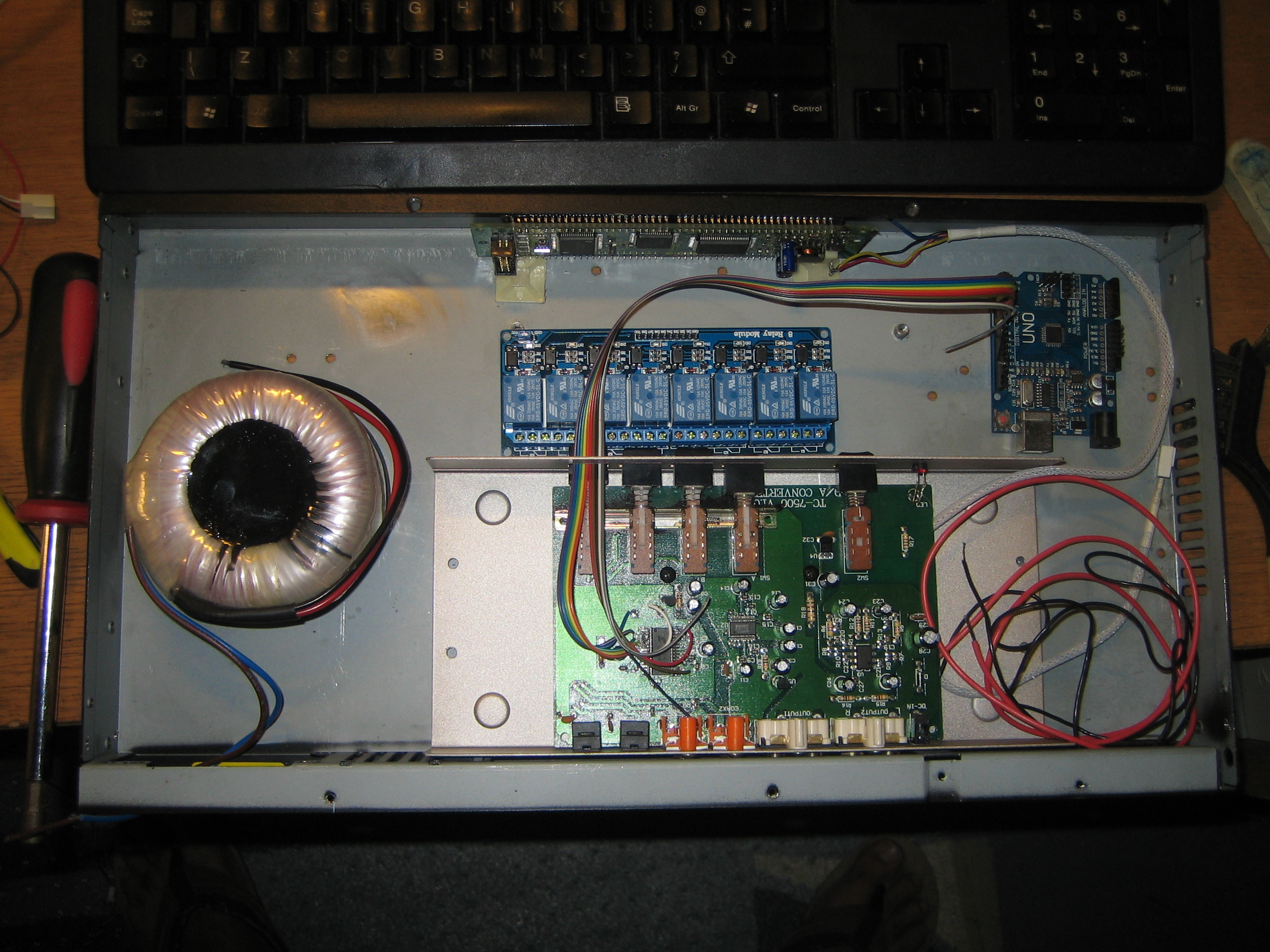
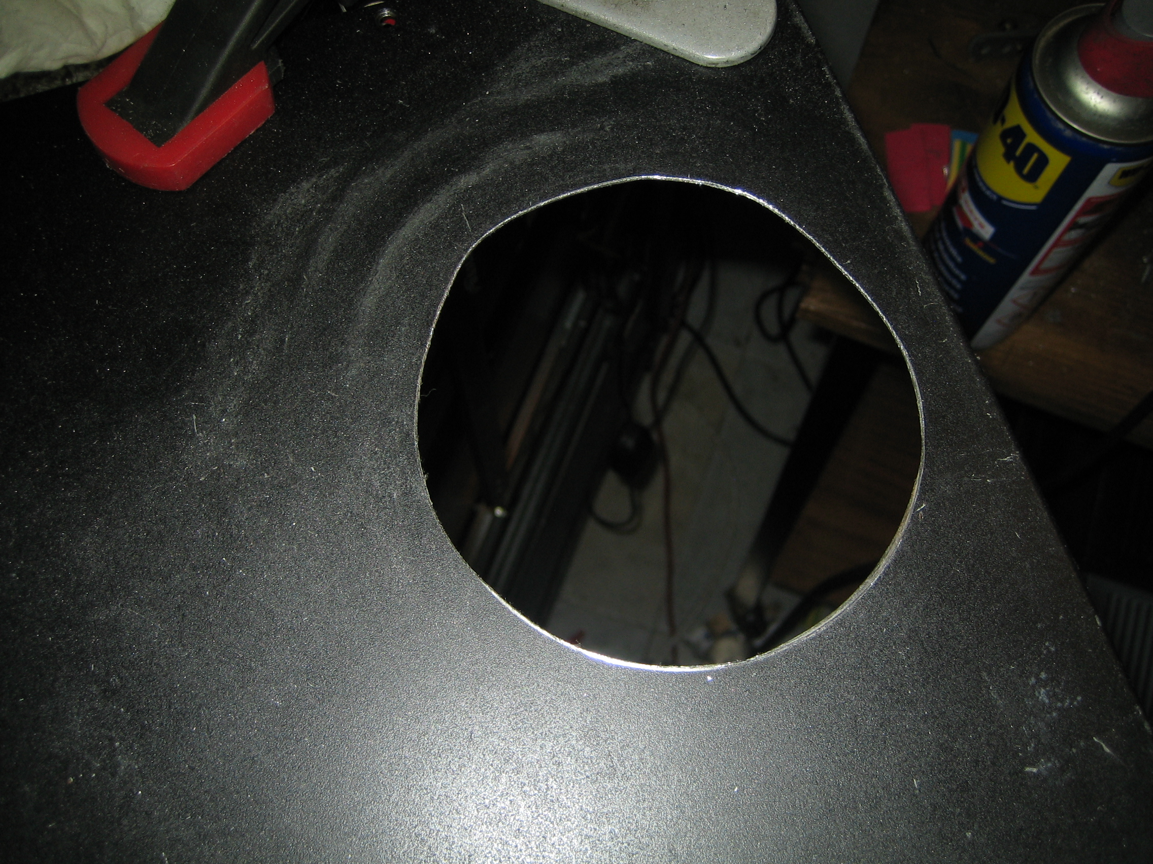
The future power supply will be on the left, with the Toroidal transformer in the centre of the horizontal. As the feet of audio devices are always in the 4 corners and the transformer is a few mm taller than the case, it is placed in this position so it does not foul anything. Due to the transformers height I have to cut a hole in the case for it.
To the right of the power supply is the VFD, relay board and DAC. We keep the relay board to DAC path as short as possible to minimise interference and we keep the original DAC case as extra ground/e.m.f isolation. The toroidal transformer produces very little e.m.f by the nature of its design (which is why it is used in Audio devices) so its closeness should not cause any major interference. Further right is the Arduino and where the other digital logic circuitry would be if needed.
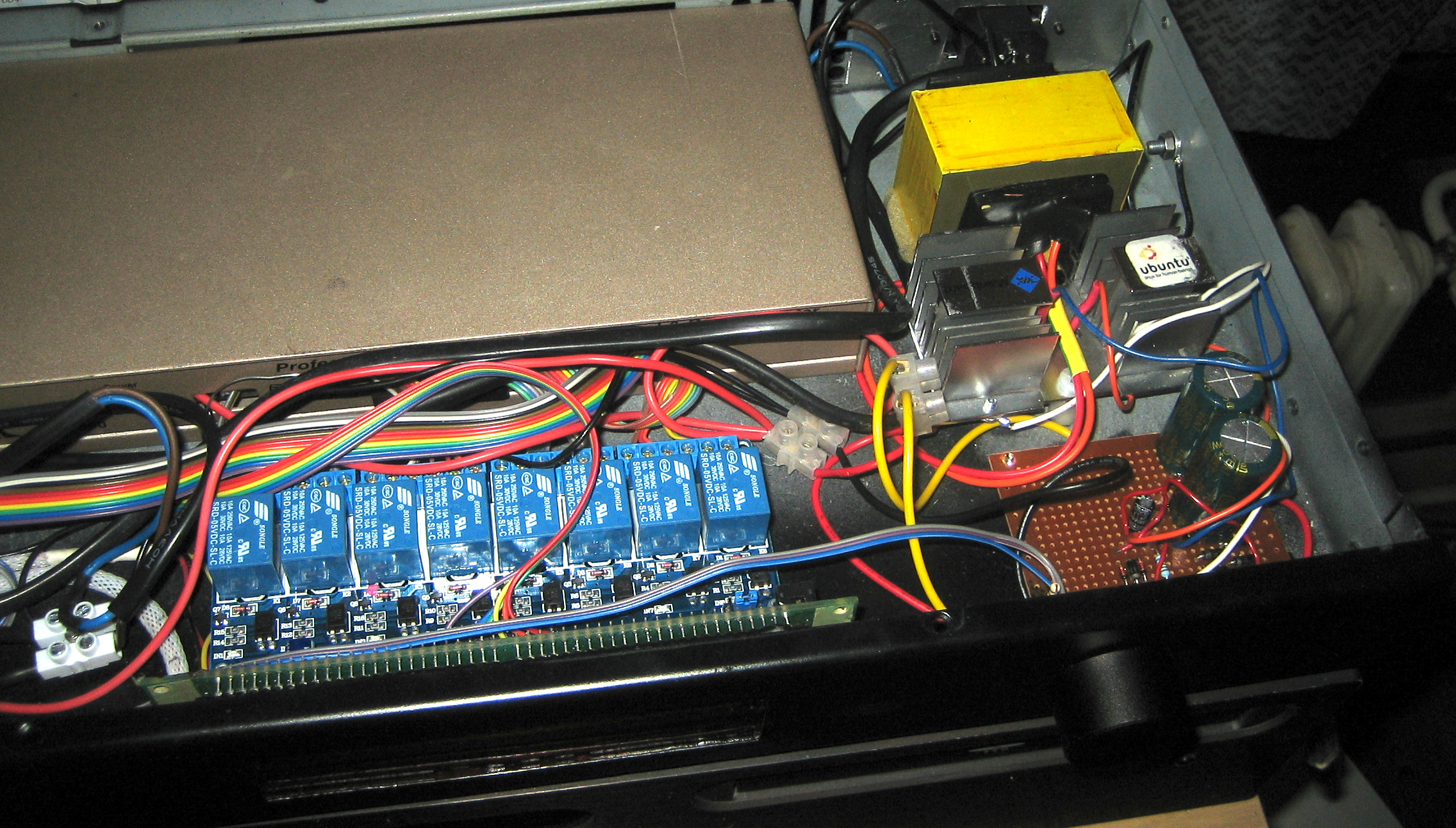
With the rough placement of components decided I marked their locations on the base of the case for future fabrication. Once placed the wiring up of the relays can begin. This was quite tedious as each of the 4 inputs has 6 pins, but compared to the SOIC it was a piece of cake. Once done they were wired to the relays and to the Arduino. Complete work as shown:
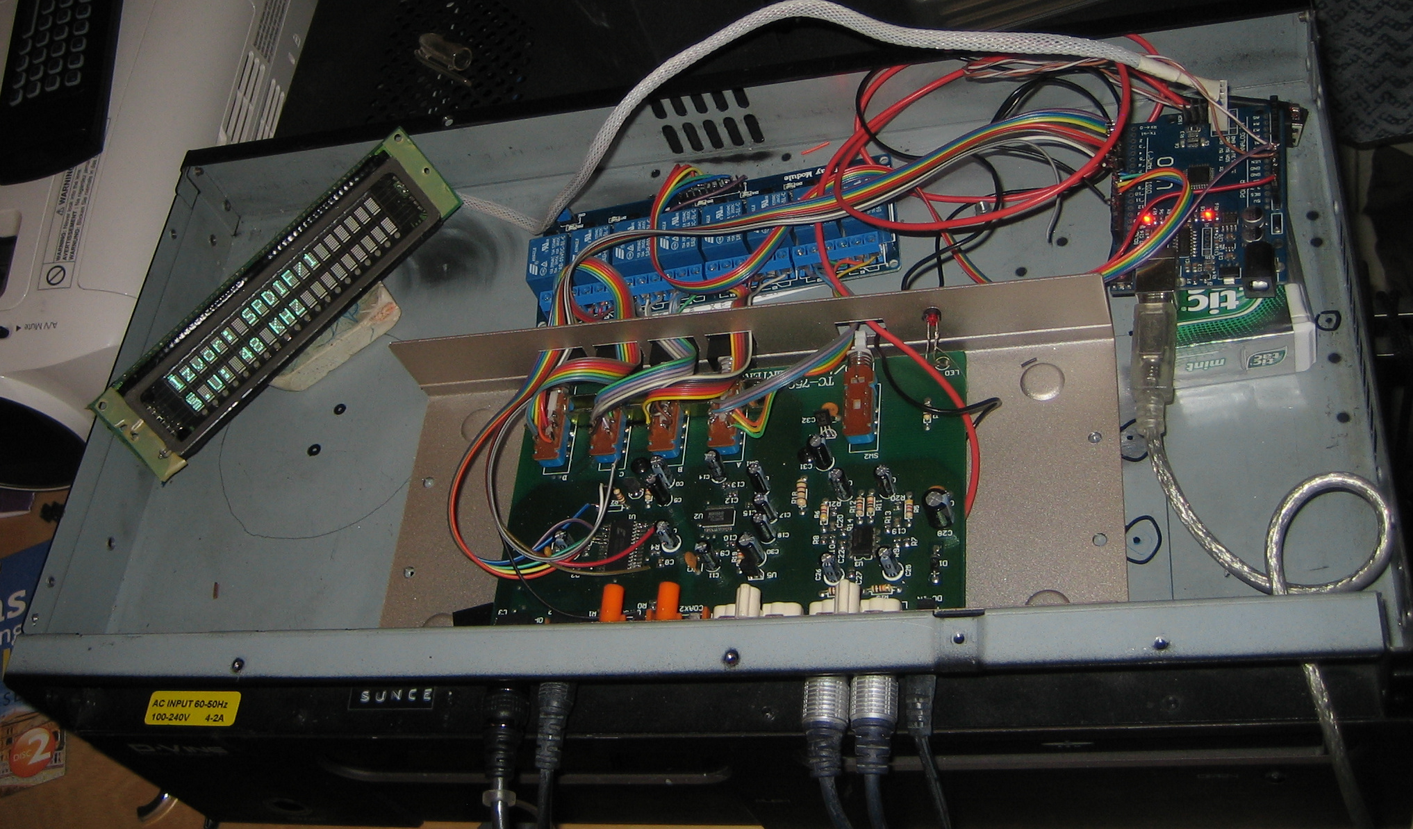
Yes, that is a piece of paper under the relays, the Arduino is sitting on a Tic-Tac box and the VFD rests on my old school rubber (that must be at least 20 years old now!). I didn't want to risk any short circuits on the bare metal of the base and those were the things I had to hand to prevent it.
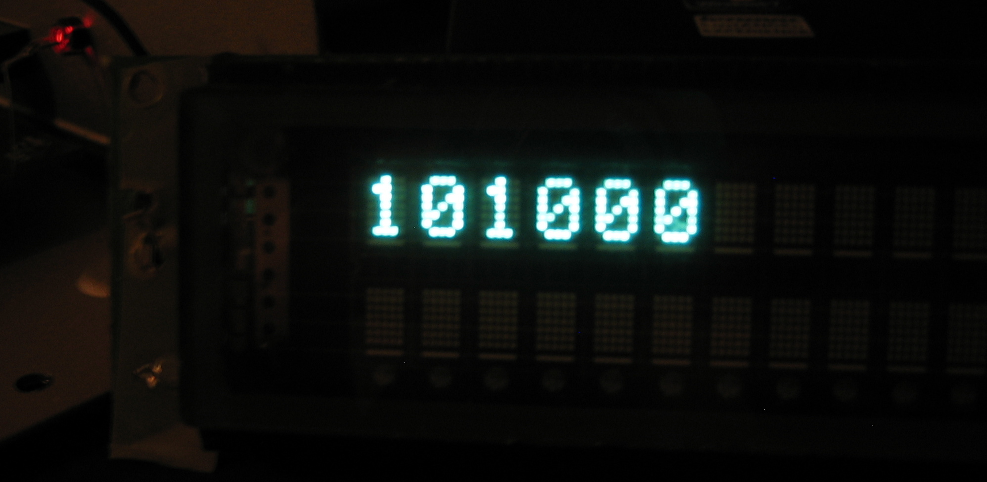
With the wiring complete the logic was written to implement a software interlock and input 1 was hard coded for testing. Now the device is actually usable as a DAC. It was placed on the Hi-Fi and plugged in. At the same time I implemented proper messaging on the VFD. It now shows the input source on the first line and either the sample rate or error message (if there is an error) on the second line.
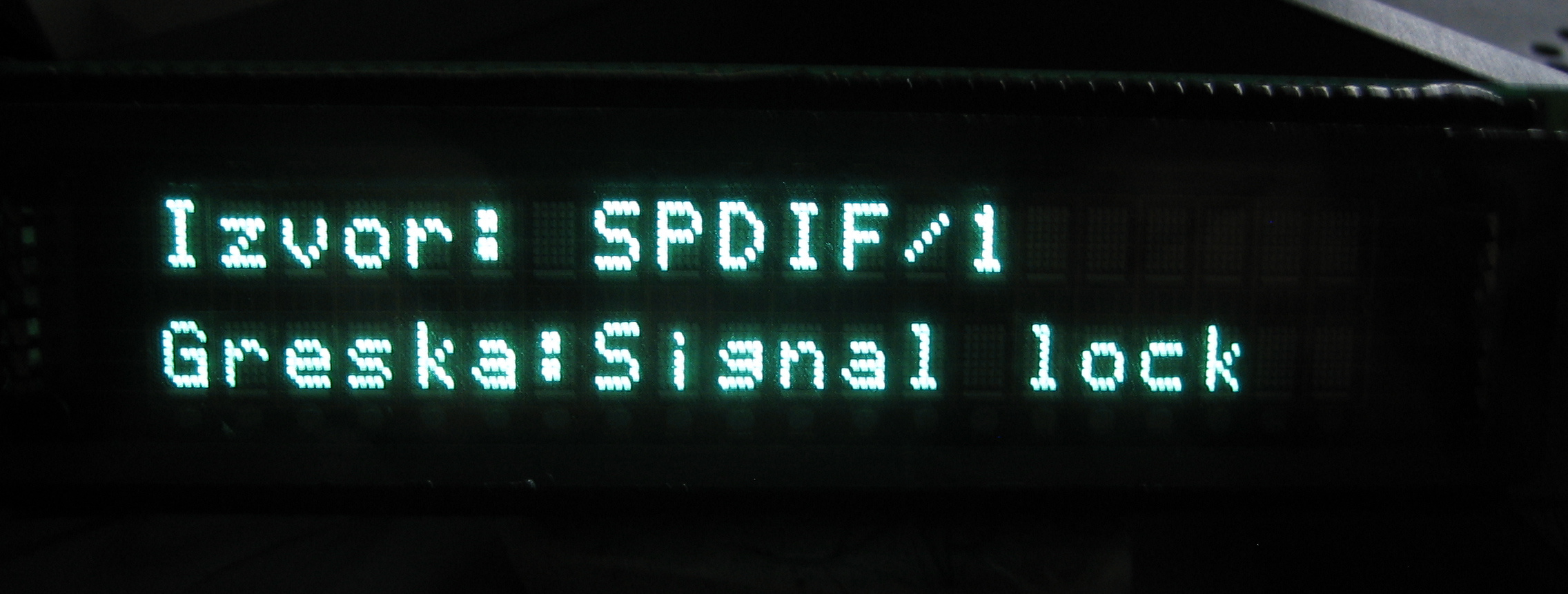
To test I would pull the input cable out fully/partially in order to try to trigger some of the other error messages. This worked and it would alert me to random errors. The only reliable error I could get is when I pull the socket out completely is the "Signal Lock" error, which was the easiest to capture:
Stage 4: Testing and Arduino firmware
At this stage we have pretty much used all the components I had lying around. The missing bits at the moment are the power button and the selector switch for which I ordered new components, as I want the DAC to have a professional finish.
Unfortunately, there are no electronic stores where I live (it is quite a niche hobby nowadays) and getting parts delivered from China takes between 1-4 months (hence why I keep boxes of junk for scavenging). As such the DAC is going to not be assembled for a while so I might as well concentrate on getting the firmware and case sorted out in the meantime.
State diagram
An advantage of using a microcontroller is that I have a lot more flexibility on what I want things to do, especially with the audio filter. Therefore my plan is to keep the filter enabled for most of the cycle, except when actually playing audio. This results in much less noise. Likewise the start up sequence makes sure the DAC has no inputs selected on power up which eliminated the occasional hissing I would get. Rather than typing it all out I found it easier to visualise the way the system will work as a state diagram:
This has now been implemented in the firmware and is running. The only missing bit is the input selector as that has not yet arrived to be installed and wired up. We also try to recover from signal errors by deselecting and selecting the input but after 3 retries it just loops from the start, as we don't want the relays constantly cycling until it gets a valid input.
Front panel
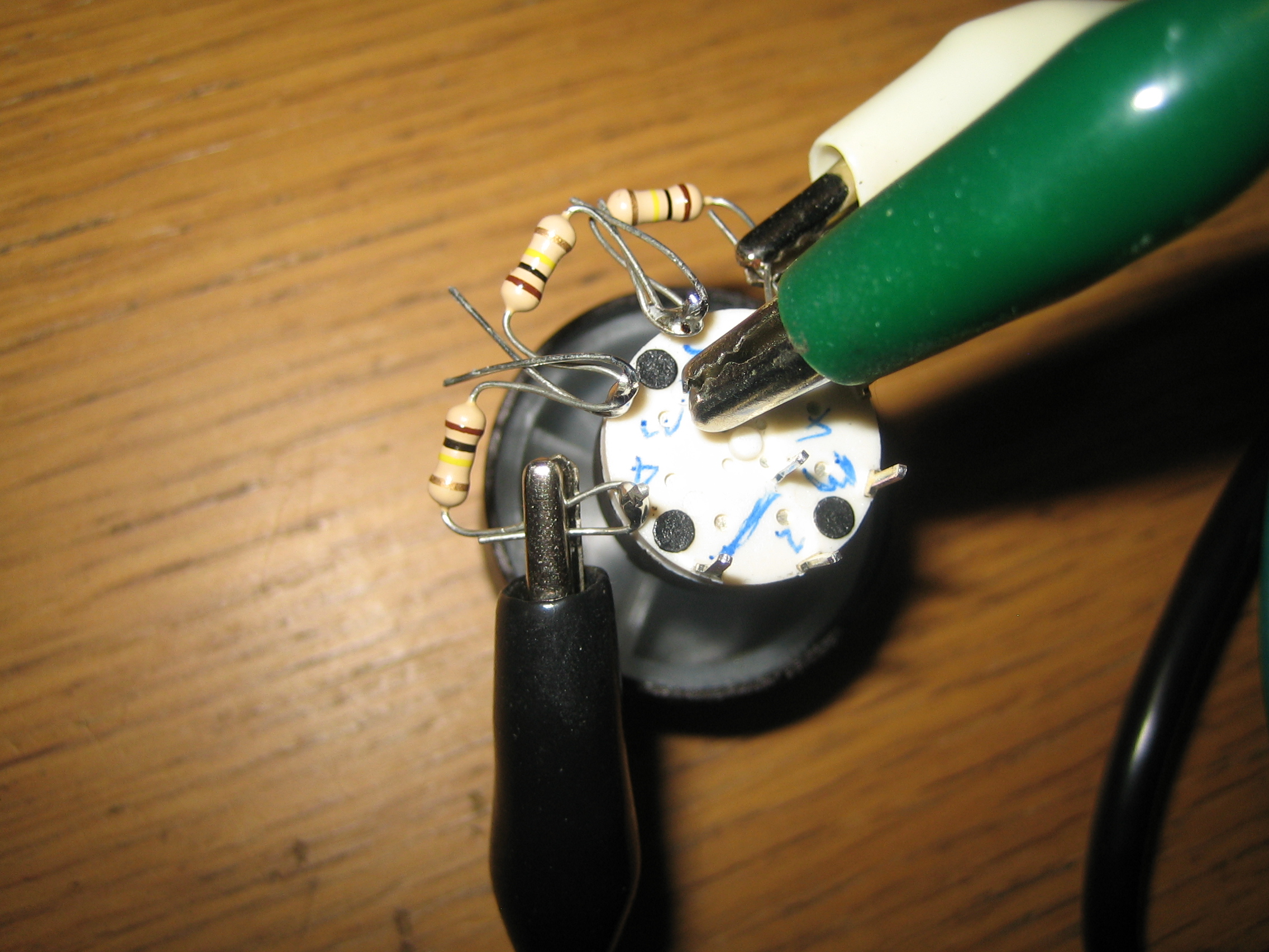
The selector switch and power button have now arrived. The selector switch has 4 positions and is dual throw, which matches the 4 inputs we have. Interfacing to the Arduino however took some thinking. We did not have enough inputs left on the Arduino for the positions. However we had unused "Analogue in" pins, so the idea sprang to mind to make use of resistance to indicate our selection. We wire resistors of equal value in series across each selector pin (as shown below) and we use it as a voltage divider, reading in the voltage through the Analogue pin. Based on that we can infer the current selection.
This design also means that the selection of input is physically tied rather than logically. Whatever we set the selector switch to, that will be our input on power on. Effectively it acts like non-volatile memory remembering the last input chosen when powered up.
The power button is a simple 240V latching switch with a LED indicator. This is wired to the mains, so when powered off the device has no power. I did not wire the LED indicator because the plan is to have it light up when in "standby" mode. Standby mode is something that I may implement in future so this is left unused for now.
Stage 5: Case mods
As mentioned above in the relay section, the case is going to need some modification. The list is as follows:
- A hole cut in the top for the transformer to poke through
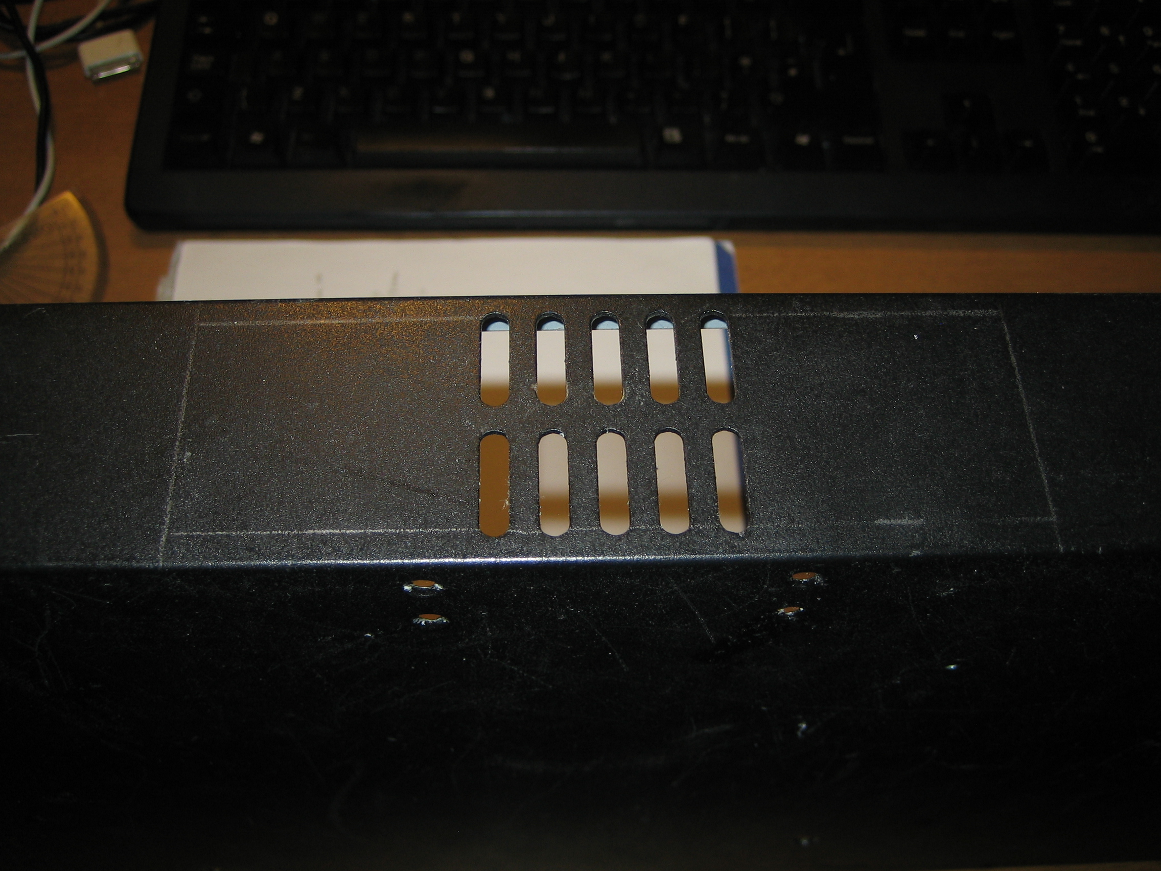
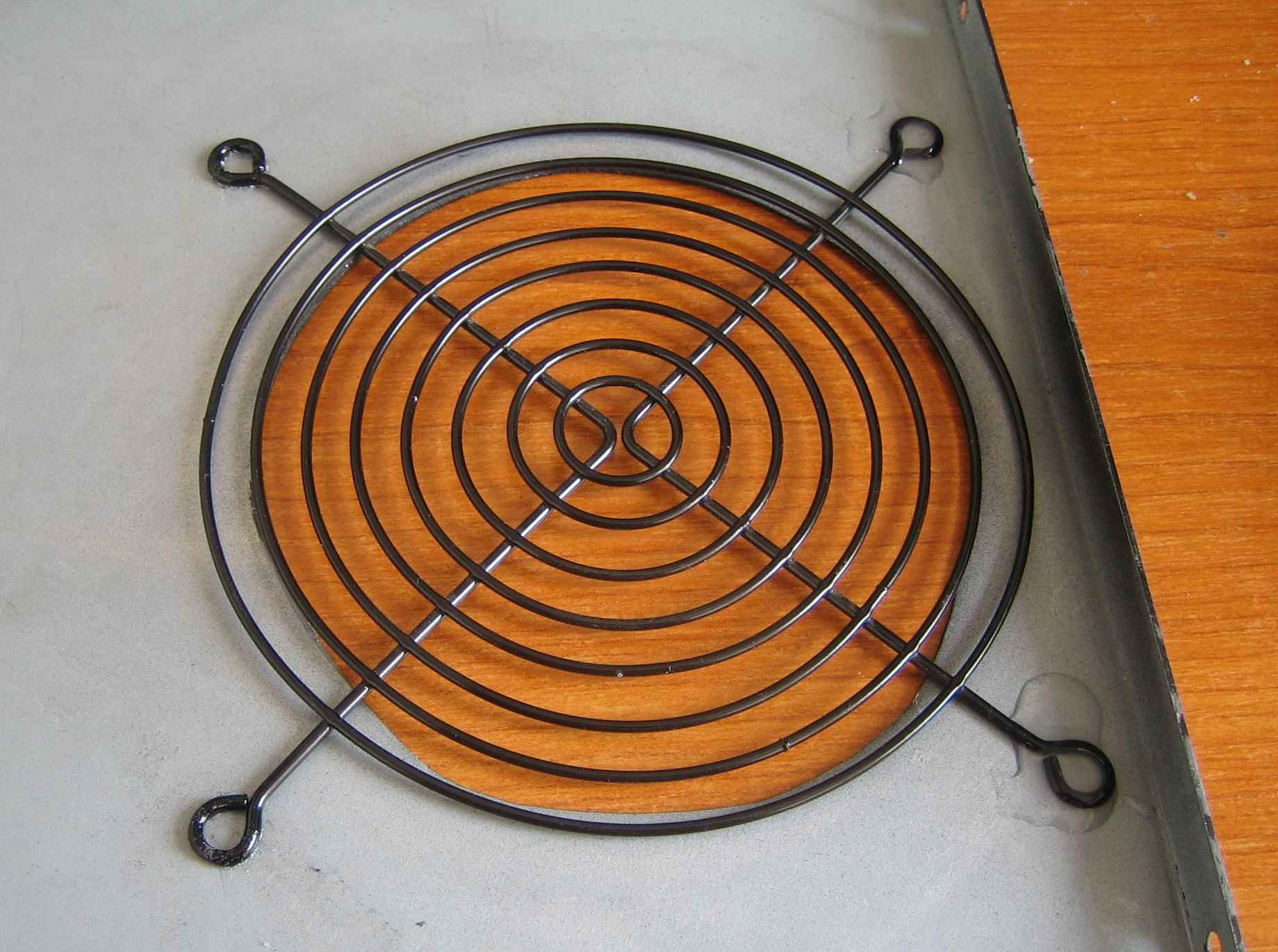
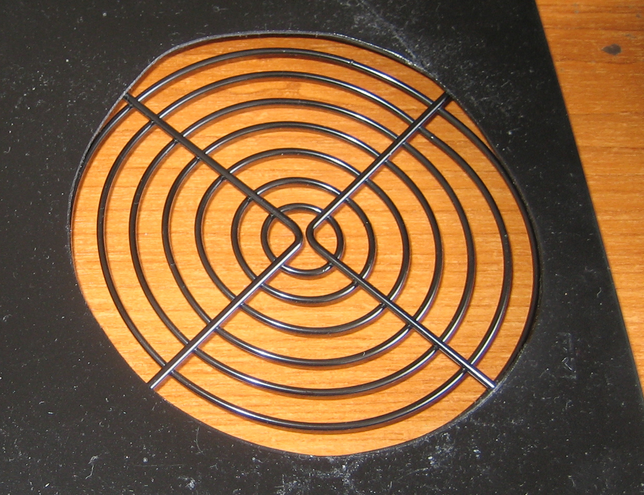
- Widening of the fan hole at the front so that the VFD can be seen fully
- Two holes drilled at the front panel. One for the selector switch and one for power
- A left mount for the rear plug and cut off switch would need to be made as well
- A right mount for the USB socket needs to be made as well
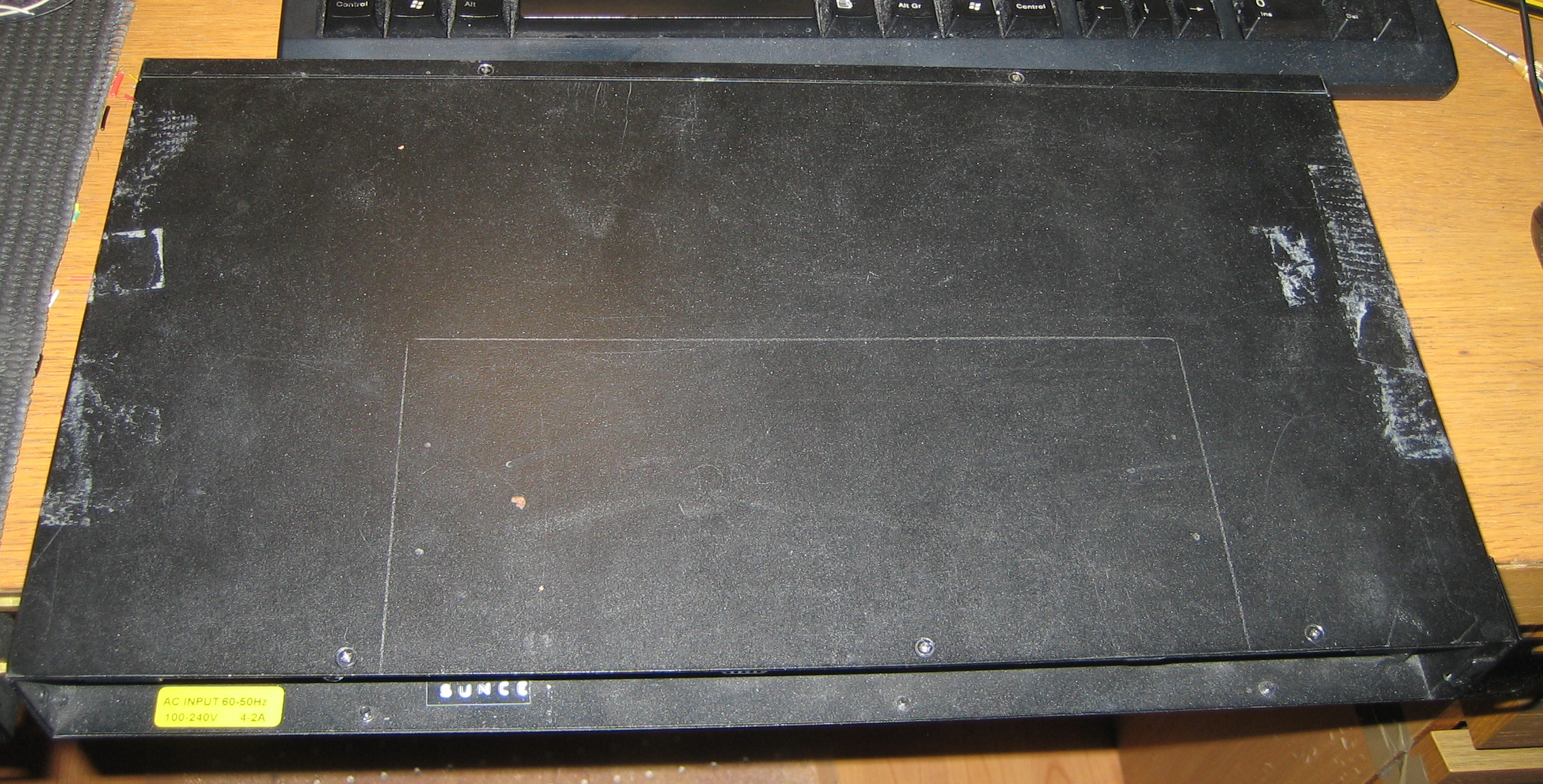
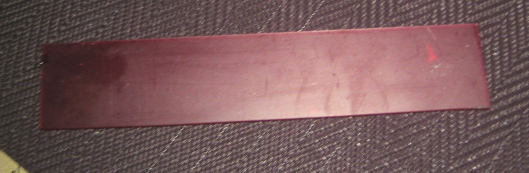
The case itself is scratched and worn as shown below, so once the above is done it will most likely be sanded down and painted. I would have liked to make it brushed steel but I just don't have the tools to make a nice brushed surface finish, so I will go with black.
First thing I decided to do is cut the front hole for the display. This involves widening the fan hole. We start by measuring and marking out where we will cut:
And then mounted it on my milling table. Here is where I realised I had a big problem. I can't detach the front of the case to cut it, so I had to mount the whole thing on the table. While I was able to fit it (barely), I could only affix the case to the table at the base. At the end we are supposed to mill from, there was no way to secure it. Therefore when I tried to mill the front, it vibrated so much I could not cut a straight line. It was useless.
At the end, I had no choice but to do it manually, using a jigsaw, tin snips and hand filling it down. The end result not only took much longer than I planned, it was not acceptable to me for equipment that would be in my living room.

As you can see without milling the fascia, I just can't make a smooth and well defined rectangle, plus the metal was warped in places from the tin snips and had to be hammered straight again.
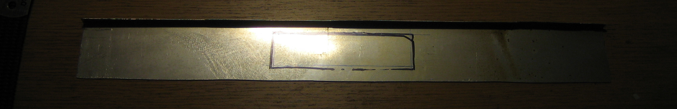
So I had to do something different. Rummaging around my junk box I found some sheet metal, which I thought was mild steel. I duly market out a template:
And got cutting. The rough cut:
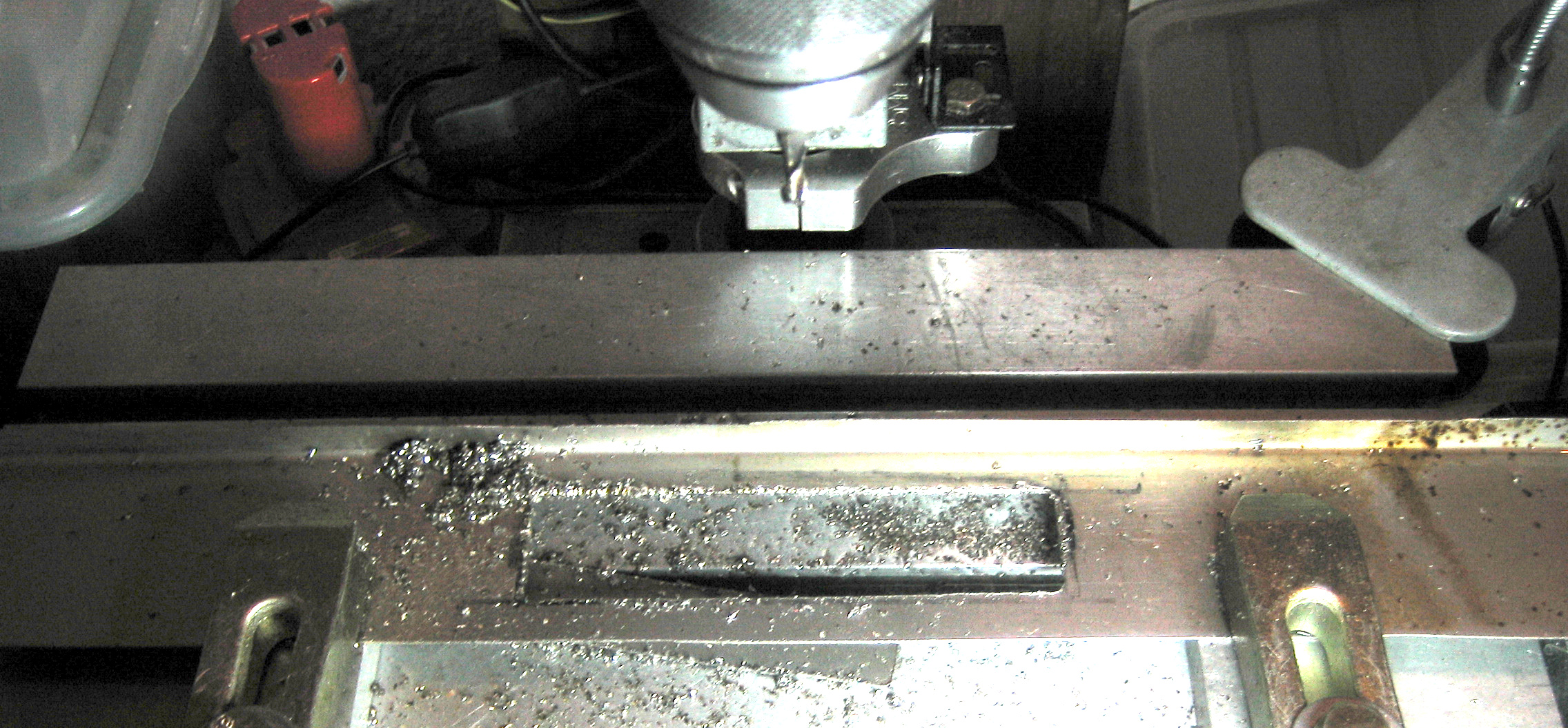
And then moved on to the milling. I thought this would be as easy as cutting. How wrong I was! It was really hard to mill and with loads of cutting oil and despite taking absolute ages (due to slow feed speed), my milling bit still discoloured from the heat. I quickly realised that this material is not mild at all. I think it is some sort of hardened stainless steel. A right pig to work with, because while being really difficult to drill and mill, its thinness meant it was really easy to bend, twist and kink, ruining the finish and the final shape.
I think this was the upper limit of what my tools can mill. In the end I managed a rough cut:
Then I hand filed it down so that it looked presentable.
Being an insufferable perfectionist I was still not happy with it (especially the kink in the right corner of the cutting), but it was better than before. I will however be painting it black because (a) it will hide some of the poorer parts of the cutting, (b) All the new parts I bought for it are black and (c) there is some odd staining on the steel that I can't seem to clean off (visible as the two horizontal lines roughly in the middle of the piece on the photo above). If I go over it with sandpaper or other abrasive tools I will ruin the brushed look anyway.
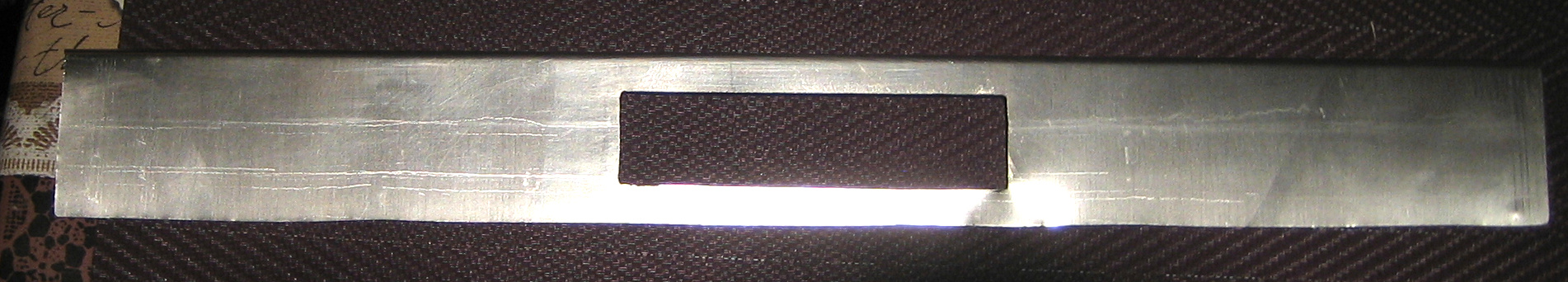
Until then, we can carry on with fabricating the other bits we need. Next on the line up is the VFD cover. I decided to go with a red acrylic because I find red more pleasing to the eye when I use the system in the dark, while still being readable in daylight. My control amp also uses red LEDs so it would aesthetically fit in with the style. Here is the piece cut out:
And the components loosely put together to test fit and looks. So far so good!

At least the fitment looks ok, I will fettle it a bit before I affix the fascia properly to the front panel.
Next bit was to cut a hole for the transformer. Being toroidal we wanted to cut a circle, that way the minimum of internals is exposed. This was another "Easier said than done" for me, because while this steel was not as hard as the front panel, it was still pretty hard and cutting large holes in steel is really at the limits of my tooling. To complicate things further, I had to make the hole a bit oval, in order to accommodate the wiring that enters into the transformer, so more manual filing down was needed. However I managed and the result was satisfactory to me:
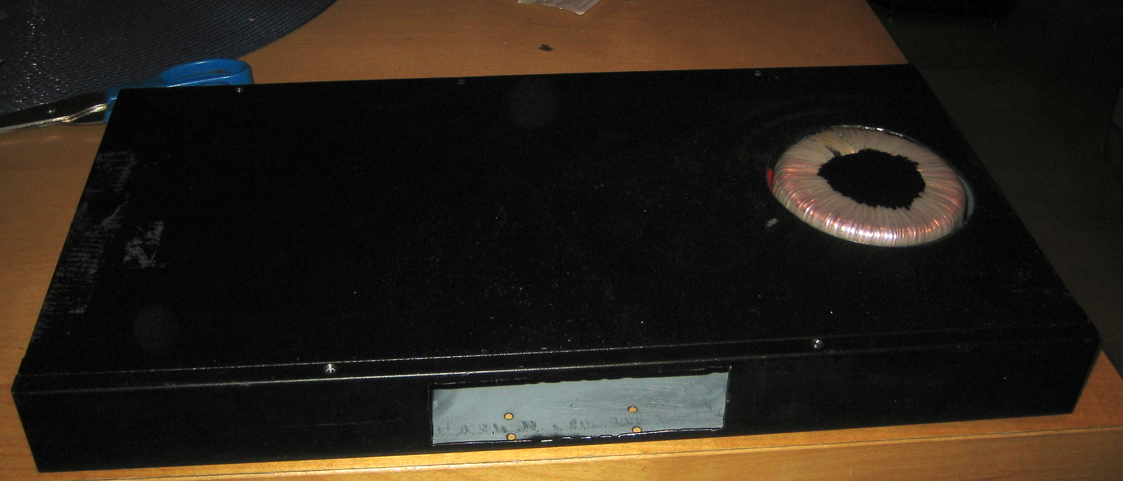
After this I started sanding down the case, in preparation for painting. The transformer sits snugly in its place, bolts at the bottom to hold it in place and the hole is enough for clearance without exposing any internals:
Next thing we did is glue the front panel to the case, further sand it down and then do the primer coats prior to painting.
The painting itself went well, unfortunately I don't seem to be able to find the photos of this step right now. If I find them, I will update this page. The end result looks the same as the "primer" photo, but in black.
Stage 6: Power supply
One goal was to avoid generation of any noise in the DAC power supply. As such the efficient switching DC-DC supplies were ruled out. I originally wanted to use a linear regulator, such as the LM317. I whipped up a quick regulator circuit for testing. While it worked fine with the DAC I found that it was unable to provide enough current. The DAC uses around 300mA which is within spec for the LM317. All I can presume at the moment is that with adding the Arduino, VFD and relays the peak current draw must be exceeding what the LM317 could provide without a voltage drop.
So instead of trying to make a power supply to my own design, I thought why not replicate the existing power supply? As I was very happy with the power supply I have been using up to now, I decided to open it up to see if I could replicate it. Probably my biggest surprise is how simple it was. As shown on the photo, we have a transformer, a diode bridge, some capacitors and two transistors.
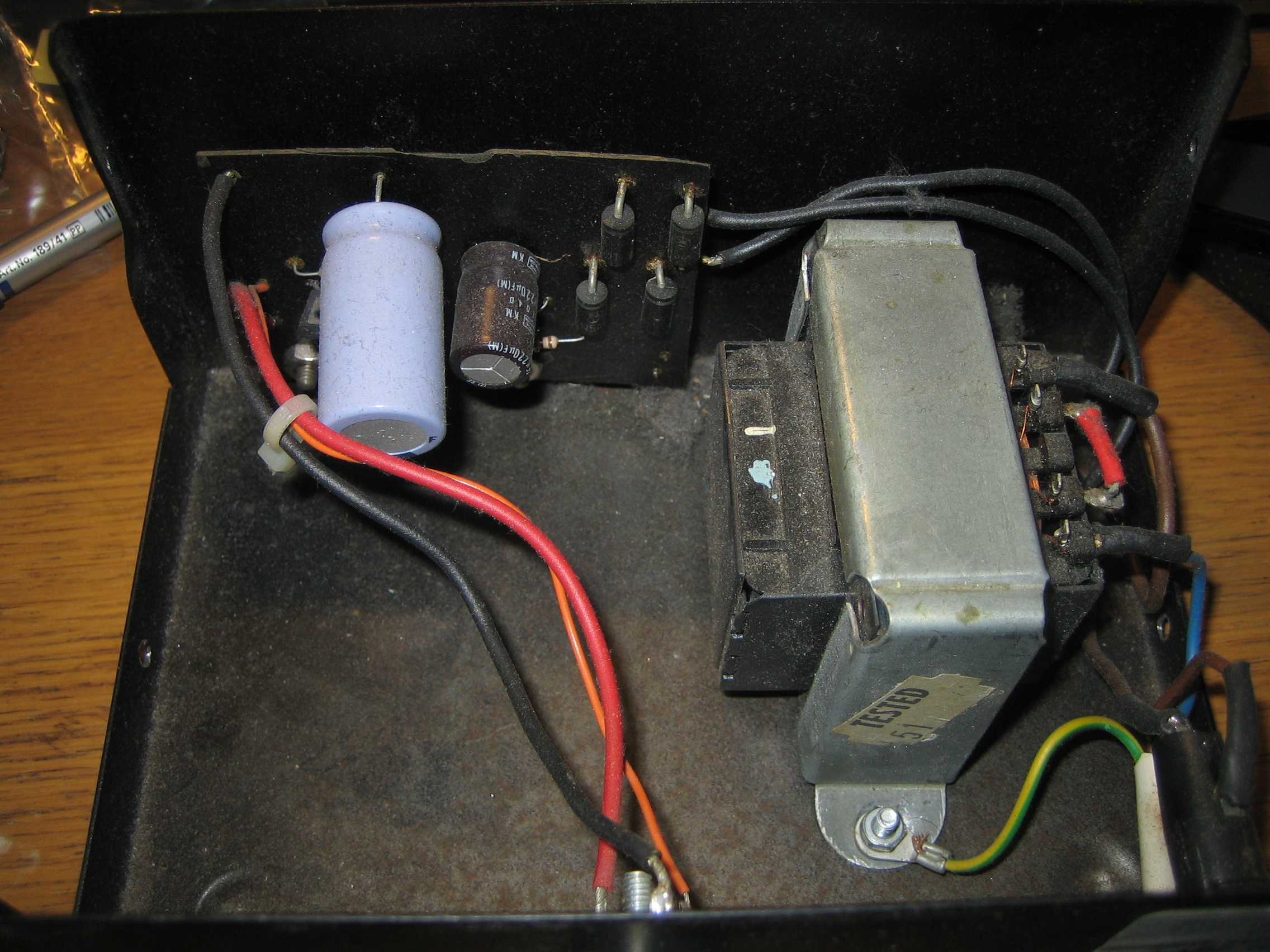
It seems that at its core it uses a Zener diode to set a reference voltage. Reading on Wikipedia brings it up as a Simple Series Regulator. The power supply is a bit different though as it looks like it has two transistors rather the one. As the Wiki page mentions it is most likely a two-stage regulator in order to reduce the impact of load on variation of output voltage.
I decided to start that I would implement the simpler version with the Zener acting as a voltage divider which goes into 2n3055 power transistor in emitter-follower configuration.
Once built and set up and tested I found a problem: the DAC audio output was very distorted. After investigating I found that the voltage was hovering around 10V, much lower than I had expected. It seems the issue is a combination of voltage drop across the transistor and the toroidal transformer voltage output. After rectification and smoothing the voltage is around 13V which after the voltage drop across the transistor is too low for our regulator circuit.
The quick fix was to find a transformer which had a higher voltage output, so I had a rummage around my junk box and found one from a old Canon Bubblejet printer, which can provide 15VAC.
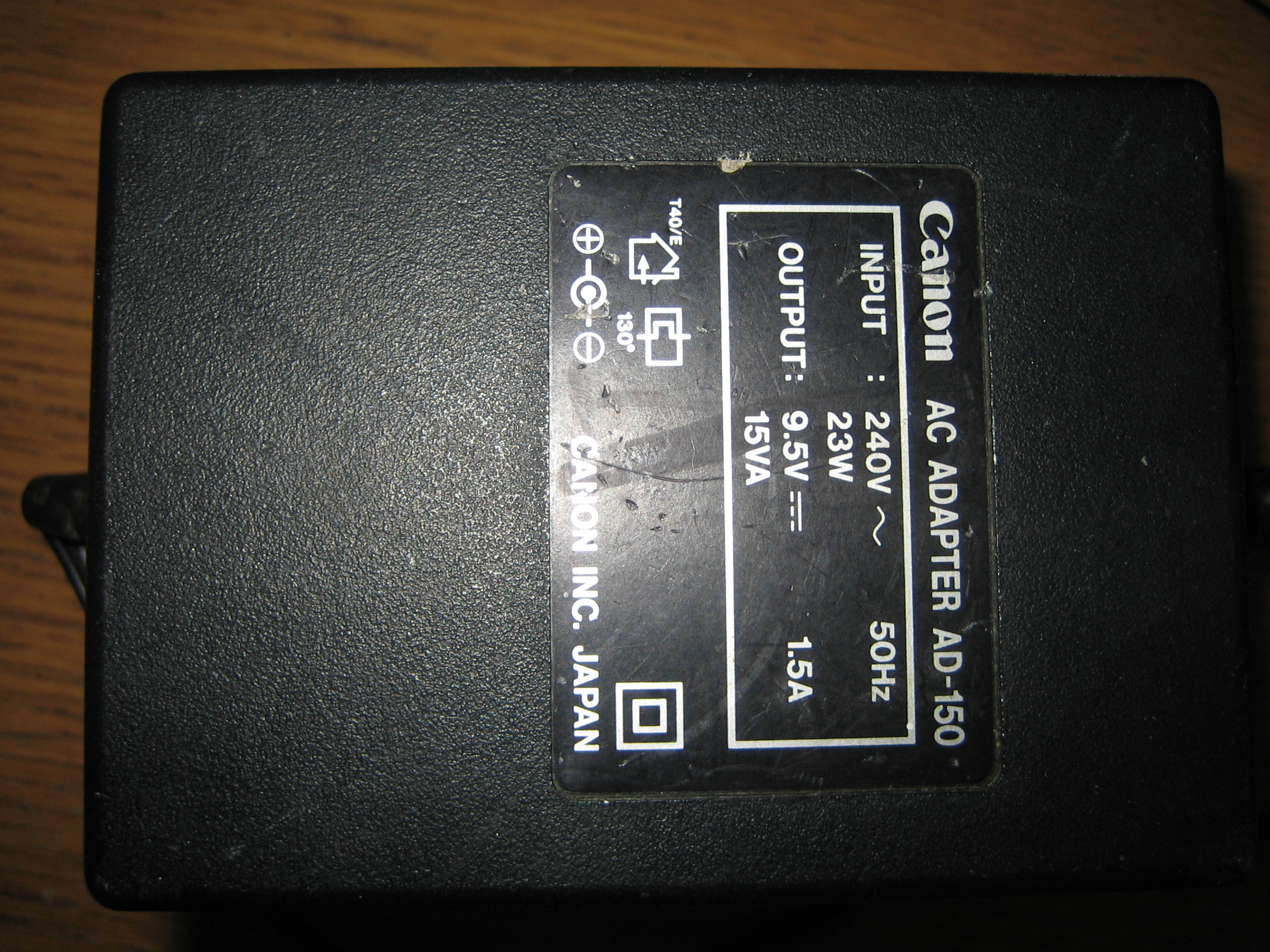
Only now, years later, do I find out why the Bubblejet printer stopped working: there was a fuse in the actual power adapter which had blown. Shame as this means the printer itself was probably fine.
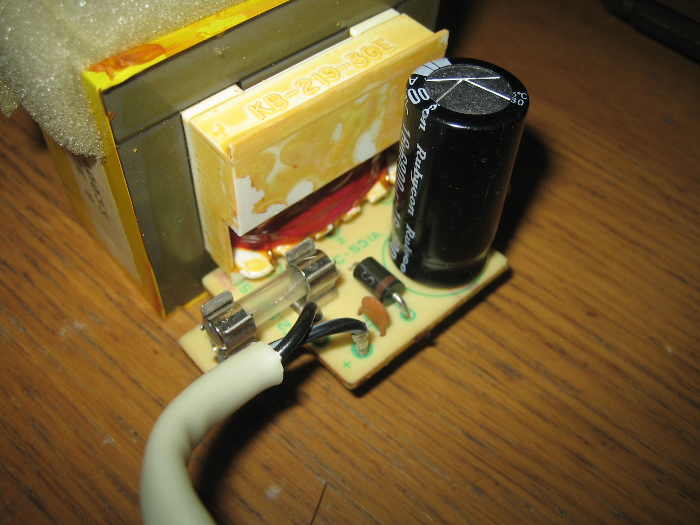
It does however mean the transformer itself has not burned out so it now gets a new life. The rectification circuit was was a centre tapped half-wave rectified which gave 9.5V DC (a very elegant design), but it is too low for our needs. So the unit was dismantled and the transformer extracted to use with our full wave rectifier circuit:
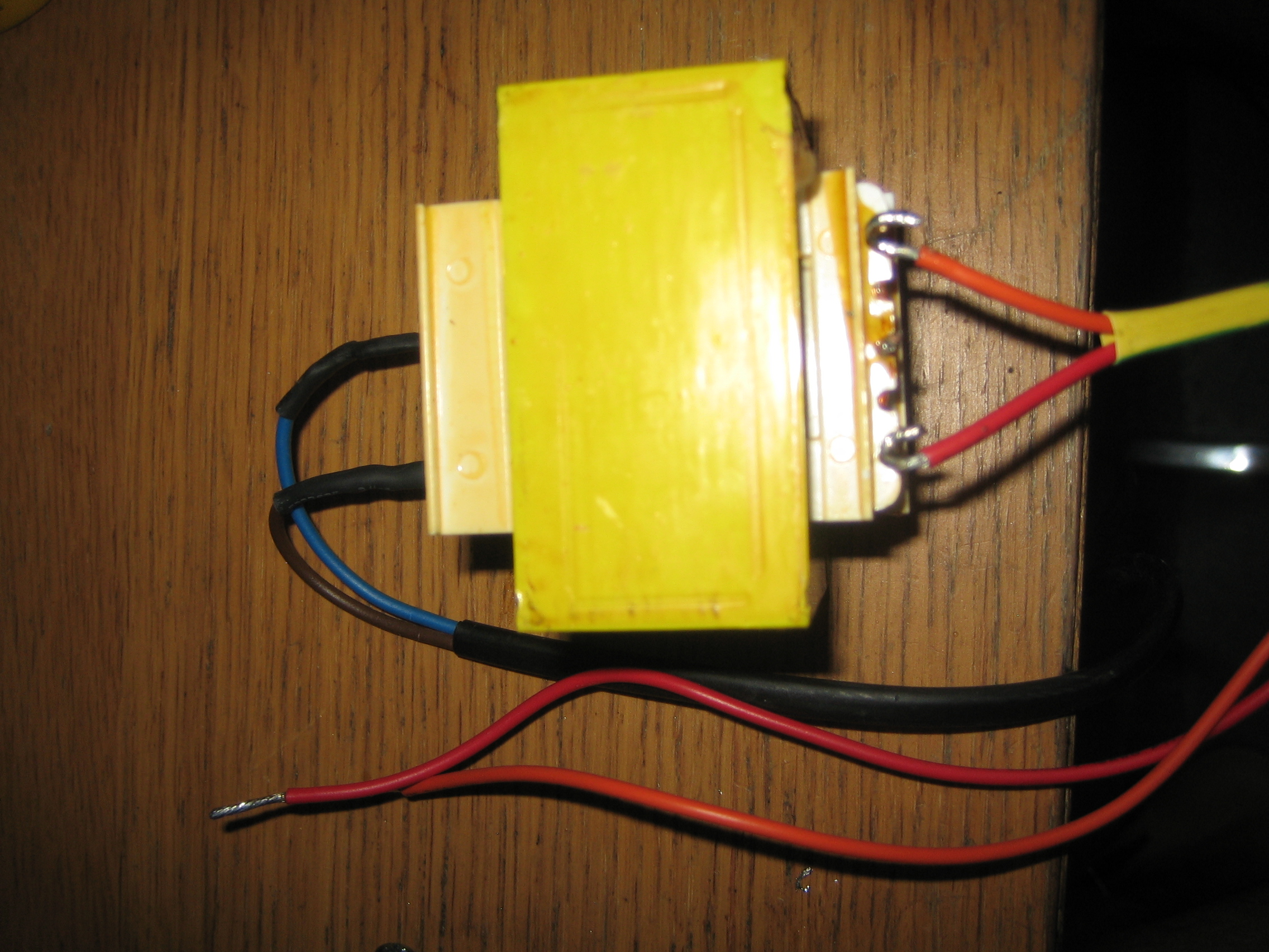
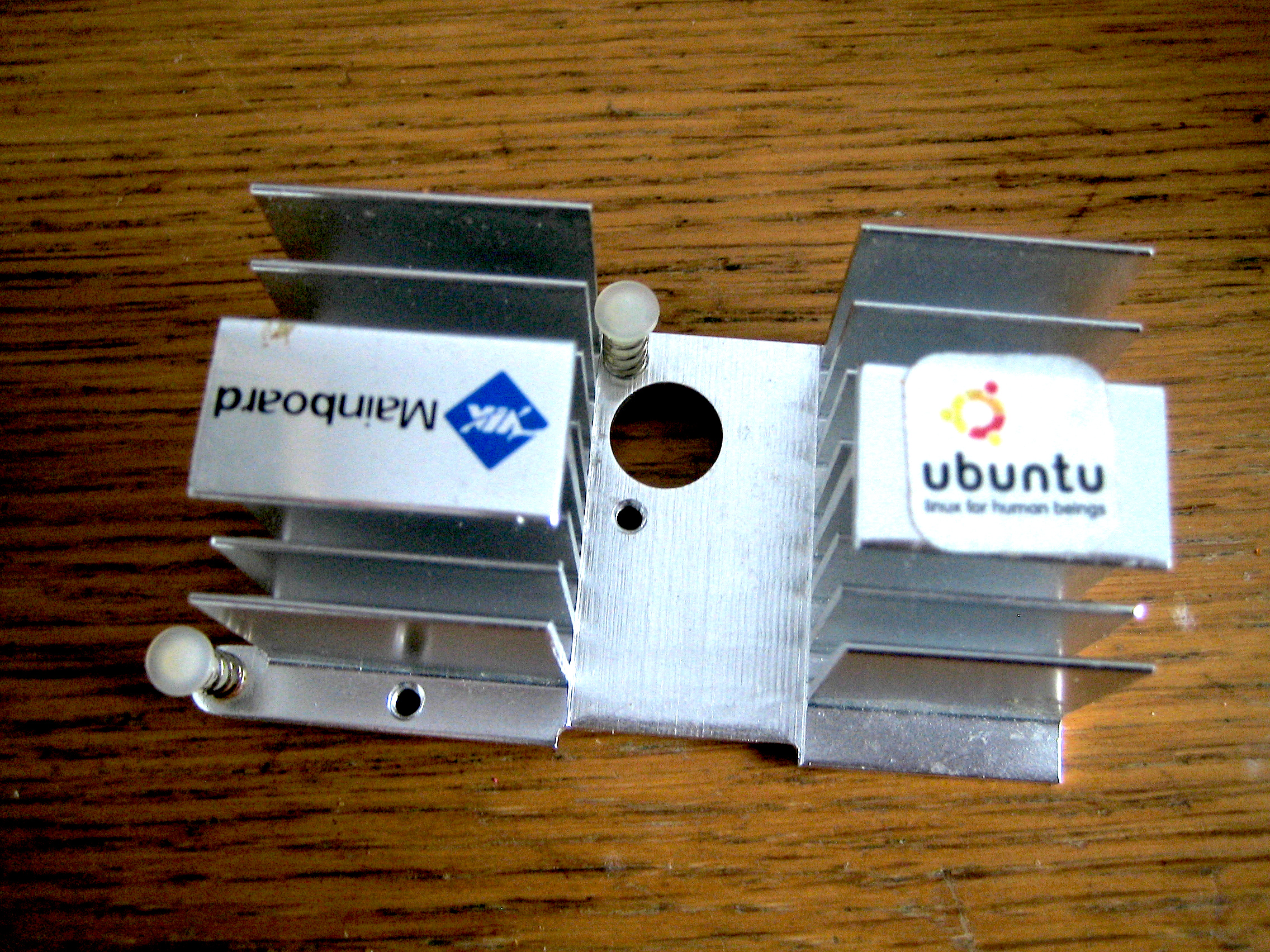
We fabricated a heat sink for the power transistor out of an old Via Mini-ITX board's bridge heat sink (shown below still sporting its Ubuntu sticker) and put it all together to test. As the transistor uses its metal case as the collector the heat sink was mounted on insulating nylon standoffs to isolate the circuit from the earthed case. Now the DAC plays audio perfectly.
The noise floor is very low which is good, however having put all the effort into making a nice oval that fits the toroidal nicely it is annoying that I could not use that transformer in the end. I can see about this in future but for now it will do. Below you can see it all positioned for fitting with the second photo showing final locations.
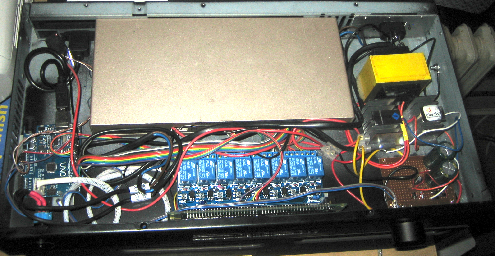
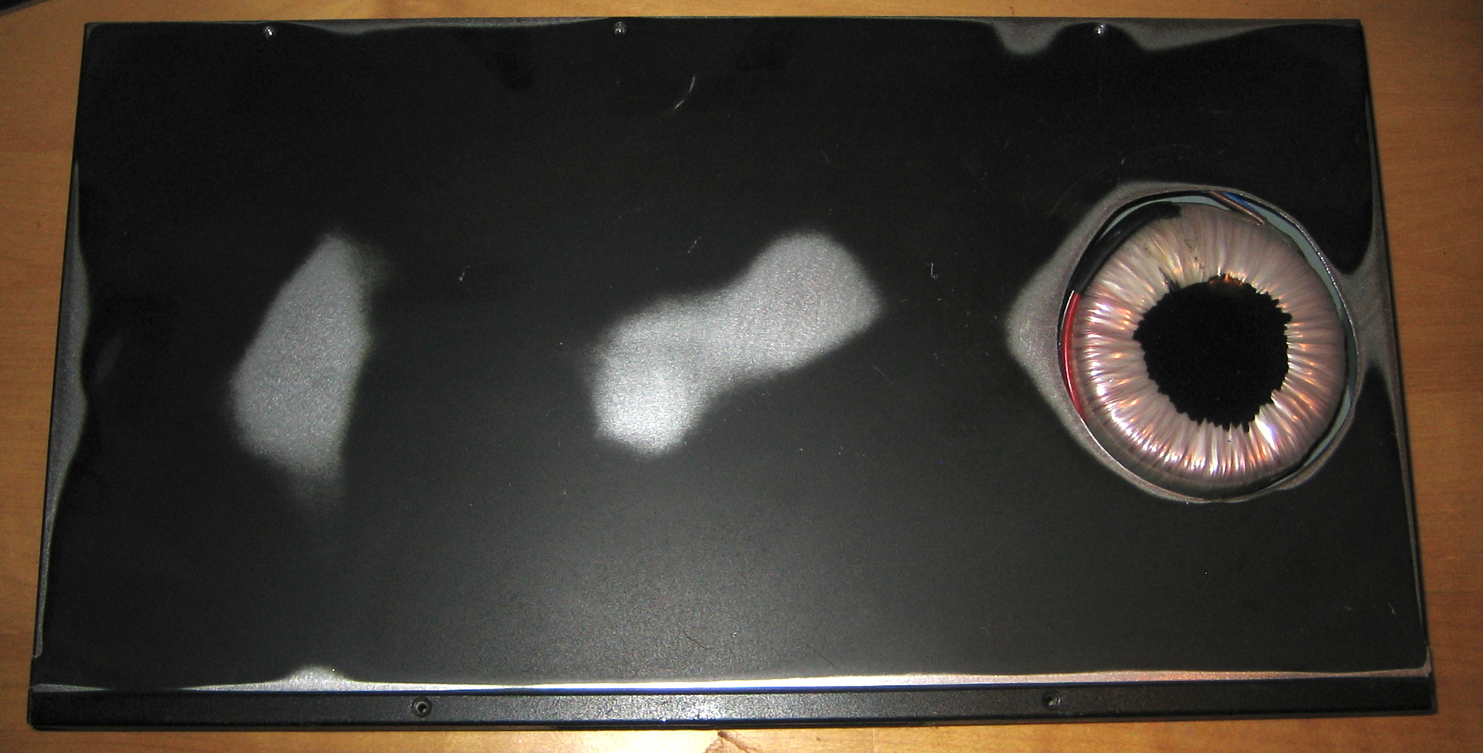
Once marked out and holes drilled to mount the components the final fitment could take place and the cover could be placed back on. I also placed a USB panel mount connector on the rear that goes to the Arduino. This will let me re-program the firmware without having to dismantle the DAC each time. The final result in the painted case:
Conclusion
On the photos above you can clearly see the new transformer is taller and much narrower than the toroidal one so the oval hole makes little sense. I made some effort to utilise it best by placing the power transistor and its heat sink in that location so it would have the best airflow for cooling. I also put a lot of effort in making sure the high voltage cables are not reachable from that area: all the cables you see are low voltage. My second worry was whether the taller transformer would foul the system stacked above, however placed with the rest of my system it looks like everything is thankfully OK. There is a few mm between the DAC and the system above it which is good.
It sounds just as good as it did before and everything works as expected. I would also say that my initial goals were met. I now have a single unit that fits the DAC and its power supply into one while blending in with the style of the rest of my HiFi. Likewise I have solved the issue of popping/hissing when starting and a modern interface with sample rate display has been made. In fact the design allowed me to go one step further and provide custom labels for each of the four inputs, which just makes the whole system feel more integrated.
Not that everything is perfect of course. The kink in the steel is still visible even after painting but that is only when the light is at a particular angle. I will admit this project ended up being harder than I anticipated mainly because of trying to machine materials that are beyond the capabilities of my tools. After the fascia was made I threw away the rest of the steel as it was too hard to be of any practical use in other projects. In future I will probably stick to Aluminium plate for projects.
Also as I was unable to use the Toroidal transformer as planned, the hole leaves us fully exposed to things falling in. I had thought about putting a metal grill on top to prevent fingers going in at least, but I worry this will in turn make that section too tall to have anything stacked above it. So I would look to see if I can make use of the transformer I originally designed the case for in future.
Either way, all that is left now is to make use of the system and see how it performs. No doubt there will be things in future I would like to rectify and the best way to find out what those are is to use the system and make notes.
June 2024
The system has now been up and running for over a year now with no issues what so ever. I've made some more changes to the software side of things, mostly just improving the display output.
As was mentioned above, while building the project I found I could not use the transformer I planned to as the regulated output voltage was too low. As the entire project was still in the process of being put together I just made do with a higher voltage transformer I found lying around temporarily.
Now that the system has been built and has proved itself well. I decided it is a good time to revisit the power supply situation.
The first step for me is to measure the voltage and current draw of the system as it currently stands. I also measured the voltage from the regulator to the transistor VDCreg and voltage after the transistor VDCtrans
VRMS = 17.4V
VDCrect = 21.4V
VDCreg = 13.4V
VDCtrans = 12.8V
AMAX = 0.3A
THEATSINK = 45.5°C
TAMBIENT = 27.6°C
In the interest of comparison I've taken a temperature measurement of the regulator heat sink with the existing power supply as well. We get a delta of 17.9°C between ambient and heat sink temperature, which is a range I am comfortable with.
From the above we can also see that we draw a maximum of 300mA of current and at that current draw we have a 0.6V drop across the transistor. We get a final regulated output of 12.8V, which is comfortably above the 12V required for the DAC to function properly.
We can also calculate the power consumption of the DAC. The equipment itself consumes 3.84W of power. However at the rectified input DCrect we are consuming 6.42W, the delta of 2.58W is lost as heat in the linear regulator as it sheds excess energy.
To make this more efficient we would need to lower DCrect to be closer to our DCreg voltage, but not so low that we risk introducing noise (the linear regulator needs some headroom in order to properly filter out noise). How much headroom? Well at a bare minimum we need it to be our target voltage + the maximum ripple voltage we see, so I used the scope to find out the AC waveform in our DC signal. From the scope results I noticed that there is an AC component in our DC signal, a ripple of around 200mV. So at a minimum we should have 0.2V higher. I would go at least 0.5V above to give some headroom.
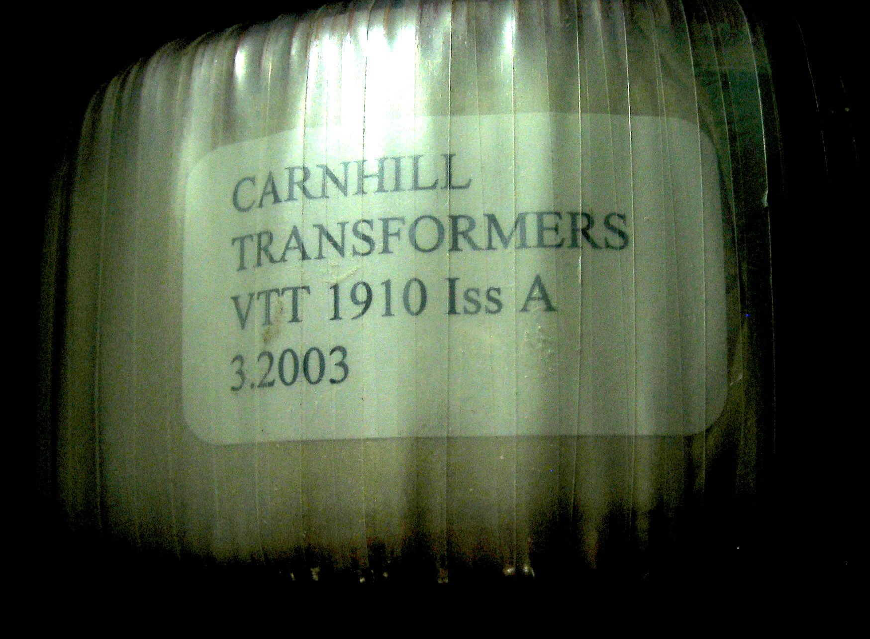
So now that we have the data points from our current system, we can look and see how things stand when I replace the existing transformer with the toroidal. First thing I did is have a closer look at my transformer. All I have to go on is the marking on the transformer of "CARNHILL TRANSFORMERS VTT 1910 Iss A 3.2003" (photo of it here).
So it is most likely a Carnhill potted toroidal transformer. The company seems to be pretty solid from their website, making a wide variety of audio and power transformers. Unfortunately this model is not listed on their website, possibly because it was a custom job or (more likely) because its old. I bought a pair of these in the mid 2000's off Ebay and you can see the date stamp of "3.2003" on it, so its just over 20 years old now. Unfortunately I found no specification sheet online so I don't know its particular capabilities, specifically its current and voltage output.
The current is not so easy to measure but judging by the weight of the unit it should be decent. The voltage is easier to discern by simple measurement. So decided to hook it up to my scope where I could see that it gave out 13V RMS. From this stackexchange link, we are told that the DC output from a full wave rectifier and smoothing capacitor is (√2 * VRMS). We would need to subtract the voltage drop (1.1V for the 1N4007 diodes I am using). I made it into the below formula and calculated for our transformer RMS output:
VDC = (√2 * VRMS) - (2 * VDROP)
VDC = (√2 * 13V) - (2 * 1.1V)
VDC = 18.3847V - 2.2000V
VDC = 16.18V (2 d.p)
So in theory it looks like our transformer should provide a high enough voltage for the system to work so I decided to build a circuit to test. I used the 1N4007 diodes and a 10,000μF 25V Electrolytic capacitor. The result was 16.84V DC measured, which is within the expected error range.
So the good news is that we can produce a high enough voltage for our needs. However our test had no load so this is the highest voltage we will see, as I expect the voltage to drop with increasing load. The next stage was to wire up our test power supply to the DAC and see what output voltage we get when under load.
The results:
VRMS = 12.6V
VDCrect = 14.11V
VDCreg = 10.5V
VDCtrans = 9.88V
AMAX = 0.3A
We got slightly less than 13V RMS out of the transformer, most likely due to the load of the DAC. The regulated voltage was 14.11V, ~2,1V drop from the unloaded test. However the big loss was in the regulator. At 10.5V output we have an almost 4V drop in our regulator circuit, not including the transistor losses which brought the final output voltage to 9.88V, much lower than the 12V the original TEC section requests.
With this voltage the DAC worked but there was an audible mains hum in the audio stage at full volume. While you can't hear it under normal listening conditions the hum was not present with the other transformer, so this is overall worse for sound quality than the existing system.
Obviously the JEC DAC itself is voltage sensitive, so the next stage for me was to hook up my bench power supply and start varying the voltage. This would assist me in gauging under what voltage range the system will operate and what range gives the least noise and best sound quality:
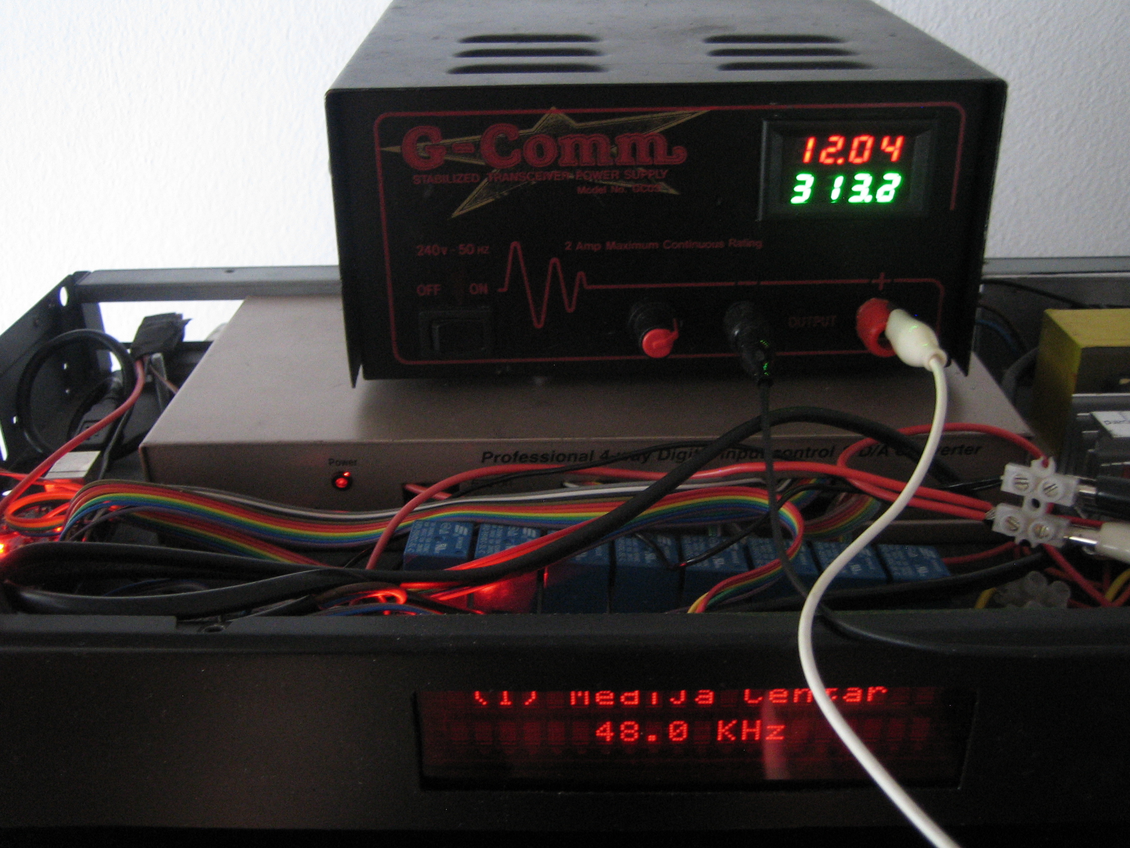
The eagle eyed of you will have noticed that my bench supply looks very much like the G-COMM I originally used to power the DAC. That is because it is the same device, once I built this project I had no use for it anymore so I converted it to a variable linear regulator to use as a bench power supply. It does a great job at this and the display shows the voltage (red) and current (green) at that instant. We now have a second measurement showing that we use about 300mA of current when running.
Having powered up the power supply and varying the voltage while having silence at full volume and music at normal volume, I discovered that the mains hum starts around 10v and gets worse the lower down you go. Likewise the current increases the lower the voltage. From 11V onwards the hum vanishes and the white noise reduces as we exceed 13V (with corresponding reduction in current draw). I also listened to distortion in the audio and found that the sound quality got better north of 13V. As such my best bet may well be to target the 13.8V the original G-COMM power supply provided.
Based on this I conclude that I cannot use my toroidal transformer, it just cannot provide the required output voltage and due to being well wrapped and potted re-winding it is not realistic. The good news is that we now know that the system works best between 13 and 14V and consumes 300mA (max) of current. This puts an upper bound on our power consumption of 4W.
The G-COMM bench power supply has a 15VRMS transformer, so we know what kind of transformer rating is good for this project. To put that into the same formula above:
VDC = (√2 * VRMS) - (2 * VDROP)
VDC = (√2 * 15V) - (2 * 1.1V)
VDC = 21.2132V - 2.2000V
VDC = 19.01V (2 d.p)
So we get 19V DC to our regulator, with the 4V drop above we have up to 15V available, which gives us a comfortable margin for our 13-14V needs.
Looking back at the original Canon power adapter I used for this system, it provides the right voltage (15VRMS) while providing 1.5A of current, much more than we need.
This means that the transformer is oversized for our requirements, but unfortunately none of the other transformers in my junk box are the right voltage rating. As such I will have to buy a new one which allows me to pick one that is more suited to our requirements, Namely at least 15V and to be physically smaller. This will remove the overhang on the top of the system and possibly allow me to cover the hole.
Having measured the height of the case at 4.2cm, I would ideally want a transformer less than 4cm in height so that there is some clearance.
August 2024
I found an old black computer fan grill that would be a good fit to cover the hole, so I glued it on the underside of the case for neatness as so:
The result is acceptable to me, as the grill now nicely covers the hole without sticking out and without any screws visible on the outside.
The only problem that I suspect was going to happen with this set up would be possible fouling against the heat sink. Unfortunately this is exactly what happened. As the grill is now a few mm below the case it hits the heat sink, preventing the top of the case from closing properly.
This can also cause a short circuit as the heat sink is at the same voltage as the collector of the transistor. Thankfully the grills black plastic coating prevents this but with time that could wear down until a short appears even if I could force the case closed. So for the moment I relocated the heat sink and transistor to the rear of the case.
September 2024
Since my last update I have been thinking that if I am going to redesign the power supply I can consider ways to reduce the noise floor further. As things stand the noise floor is already below every single audio file I have played so this is not critical, but more of a nice to have.
Most of the noise you can hear is white noise which I suspect is RFI from the microcontroller power supply. I am powering the Arduino from a small 5V USB supply connected directly to the 5V pins. This is very efficient as it bypasses the Arduinos regulator but (a) I suspect it adds noise and (b) the risk of a power spike will fry the Arduino and other connected components as there is no protection. While the Arduino and relays are easy to replace the VFD would be difficult. It was made in 1997 and finding another one that would fit the design would probably not be easy.
Arduino themselves recommend you power the microcontroller through the jack which is protected and has a built in regulator, allowing for an input voltage range between 7V and 20V. This means that I could remove the 5V DC-DC converter and power the Arduino straight from the 13.8v regulated power supply.
The thing is that powering the control system via the jack will be less efficient so I suspect the total power consumption would go up. To check this I wired the digital control circuitry to my PSU via the Arduino jack and measured the current draw at 15V. I got around 450mA, of that ~300mA is the VFD itself while ~80mA is the Arduino and relay when holding. When switching it briefly spikes to almost 200mA. Therefore if we are to power this from the main power supply then we need at least 800mA to be comfortable.
If we design the new power supply to provide 1A at 15v maximum, we would be looking at a power draw of 15W
This gave me an idea of the kind of transformer sizing I will need. A transformer that is less than 4cm in height but can fit in the existing area while providing around 20W would do.
I had a perusal online of options and I found that most transformers above 5W were toroidal. I found two potential toroidal transformers, one 15W at 15VA (30x35x75mm) and one 30W at 17VA (30x35x75mm). I admit I don't quite understand the dimensions as I would normally expect such transformers to have a radius/diameter and height. I assume 75mm is the diameter and the larger of the remaining numbers is the height. At 35mm we are still 5mm below our maximum and 75mm is within the free space in the enclosure. Considering they are almost the same size I would rather go for the 30W one so there would be plenty of headroom for future power requirements, despite the higher voltage meaning we will have less efficiency (more energy will be dumped as heat). Delivery is expected end of November, so this is likely to be a December project.
The good news is the 2n3055 I am using can handle up to 15A of current (and a temperature of 200°C) making it still the best candidate for our power supply. The alltransistors.com page has the details for our transistor, so given the new load we can calculate the ideal resistor to use with our zener based regulator:
First we need to calculate the VDC that will be entering our circuit. As the new transformer is 17V RMS the DC output should be:
VDC = (√2 * VRMS) - (2 * VDROP)
VDC = (√2 * 17V) - (2 * 1.1V)
VDC = 24.0416V - 2.2000V
VDC = 21.84V (2 d.p)
The details of our load and transistor:
DAC = 200mA @ 14V
Rest = 500mA @ 5.2V  # Below 5.2V the VFD became erratic
ICmax = 1A  # 0.8mA measured plus some overhead
# Below taken straight from 2n3055 datasheet
βmin = 20 (@IC = 4A) # Some datasheets mark this as hFE
βmax = 70 (@IC = 4A)
VCE = 45V
Given the β range of 20-70 at 4A, I am going to presume at 1A it will be near the βmax of 70, so I will use that value.
IB = 1 / ( β + ILOAD)
IB = 1 / ( 70 + 1A)
IB = 0.01409A (14.1mA)

R = V / I
R = 21.84v / 0.01409A
R = 1,550Ω ≅ 1.5kΩ
October 2024
The transformer has arrived, much faster than the November estimated time. I can confirm the measurements they gave me is the outer ring diameter (7cm), inner ring diameter (3.5cm) and height (3cm). The transformer is much smaller than the previous toroidal I intended to use so there should be plenty of room in the case. In addition the transformer is centre tapped 17v-0-17v, meaning I only need two diodes to make a full wave rectifier.
Based on the calculation done earlier our ideal resistor would be 1.5kΩ. Looking at my choice of Zener diodes I have 12V and 15V. The 12V is too low (as we will have a ~0.7V drop across the transistor) so I've decided to go with the 15V Zener. I've put together this basic schematic of how I expect the PSU to look:

The use of the 15V Zener should give us an output of 14.3V and would dump an excess of 6V at 300mA (1.8W) as heat when in use, which is within acceptable parameters. 14.3V is also within the 7-20V range of the Arduino power input and as tested earlier should give us good output from the DAC as well, albeit 0.5V higher than the 13.8V of the original PSU. The LED and resistor not only provide an indicator that the circuit is powered on, but it also helps discharge the circuit when off. With that I started work on the prototype power circuit on a breadboard:

Testing of the prototype went well, giving us 14.25v and thereby validating our calculations above. Next step was for me to verify that it works with the existing system. While the DAC is happy with a 14.3v input I discovered a problem with the Arduino. It would power on but after a few seconds would start cutting out. After looking online it turns out the problem is with the Arduinos regulator. While it accepts a voltage range of 7-20V and is rated to supply 1A of current, it can only do so up to 7.5V. At higher voltages the 5V regulator gets so hot the thermal cut out triggers, which is what I was seeing. I wish this was better documented as when Arduino said that it can take 7-20V up to 1A, as the implication is that you can pull 1A of current from it at 20V input. Anyway, this means the original switched DC-DC module will remain for now. Once testing was done the power supply was installed in the case:
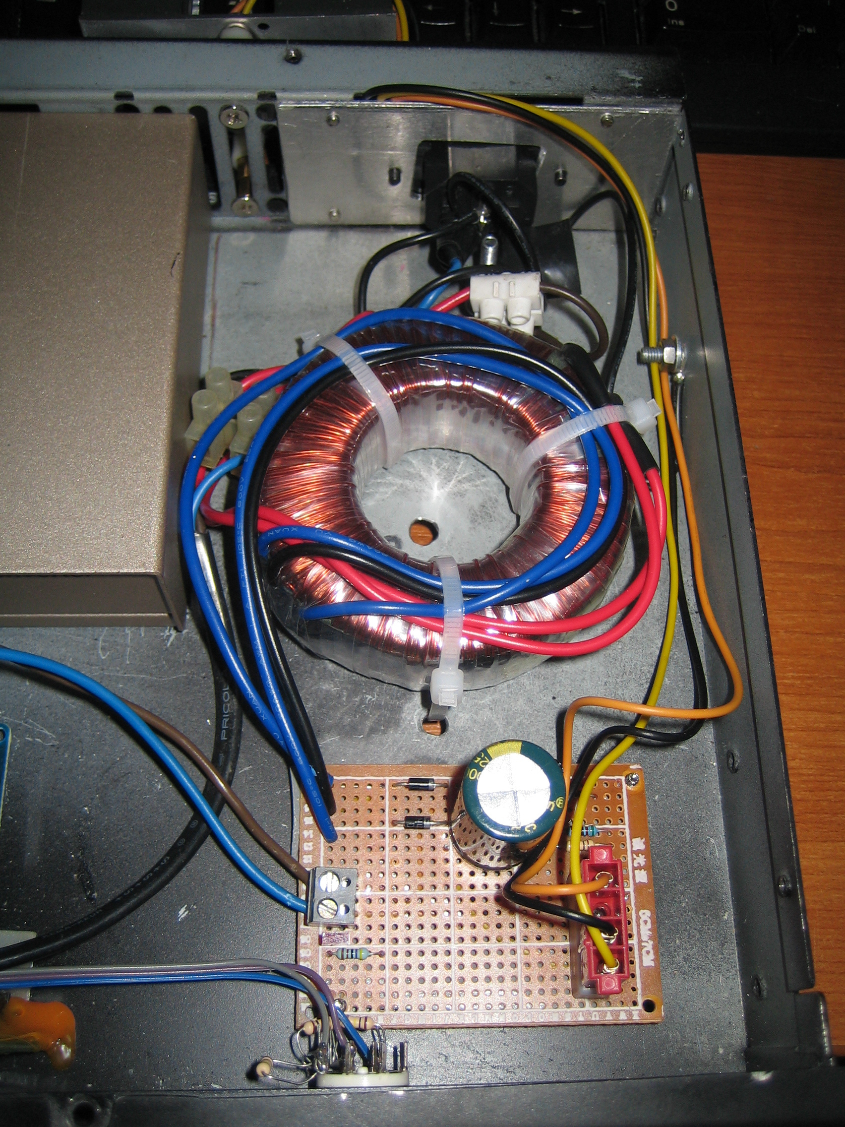
With the new transformer there is no more space for the heat sink inside the case, so the outside set-up is going to remain for the foreseeable future. I added a 4-pin Molex socket and connector to allow me to disconnect the transistor when I need to thread it through the case to the outside. The circuit itself is quite compact meaning there is space on the stripboard for future needs. Unlike the previous transformers that had mounting lugs this one does not, as a result I decided to use cable ties to tie it to the case, while also tying the wiring down so it would not protrude through the grill.
With the new set up I once again took temperatures of the heat sink so see the temperature delta:
# 2h run test, 5 samples taken and averaged (mean)
Ambient temp: 25.5°C
Heatsink temp: 37.9°C
Δ temp: 12.4°C
As can be seen the delta of 12.4°C is lower than the 17.9°C delta of the previous system, meaning less heat is being lost in the power supply. Of course this may well be due to the higher output voltage, meaning the regulator in the DAC and Arduino may be generating more heat from their own regulators. Considering the DAC was not getting the full voltage it needed to run well I expect that overall there is less energy loss due to heat in the system.
As for the sound, I can say it sounds good. The improvements are minor (as is expected, the more you refine a system the more effort is needed for smaller gains) primarily noticed as a reduction in distortion in the high frequencies. However the main goal of this update was to improve the packaging by replacing the transformer, which was completed successfully. Hanging the transistor out the back does not look like it will be a big issue for me. Not only is it not visible unless you look behind the DAC its cooling should be better than when it was inside the case. I am happy to leave it as is unless something requires a change in future.


